TSMC: 7nm Now Biggest Share of Revenue
by Ian Cutress on January 17, 2019 9:00 AM EST- Posted in
- Semiconductors
- TSMC
- 7nm
- CLN7FF
- Revenue
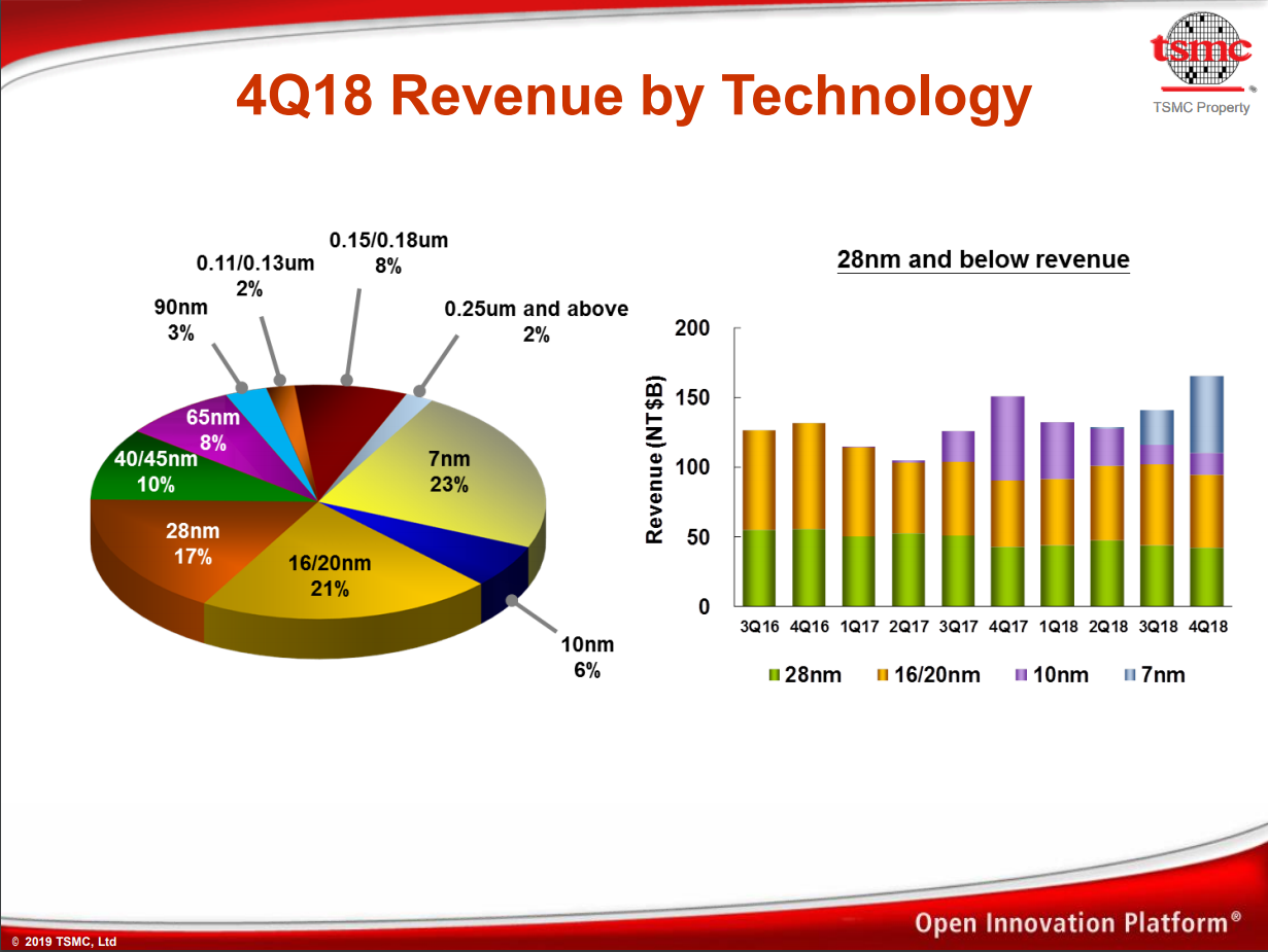
As process node technology gets ever more complex, it costs big dollars to develop and then building chips on the process is also a very costly process. The big foundries often have many process nodes running in parallel across a wide range of price brackets in order to both diversify the revenue streams but also offer multiple competitive options for the market. The latest numbers out of TSMC are stating that in Q4, the revenue generated from their leading edge 7nm node family now takes the biggest percentage of revenue for the company.
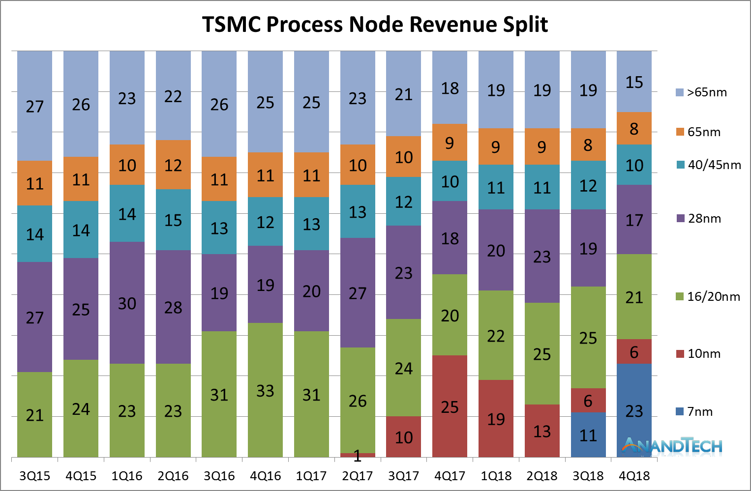
As posted by David Schor of WikiChip over Twitter, taking data from TSMC’s earning calls over the years and adding its latest Q4 results to the mix, it shows that 7nm has had a significant ramp, becoming 23% of the revenue of the company since it starting offering it as a process. Over the course of 2018, TSMC has stated that 7nm has accounted for close to 10% of total revenue, and the company expects the process node to be worth ‘greater than 20%’ of its 2019 revenue.
In the Q3 earnings call, CC Wei from TSMC stated that:
This is the first time in the semiconductor industry the most advanced logic technology is available for all product innovations at the same time. We continue to work with many customers on N7, N7+ product design and expect to see more than 100 customer product tape-outs by end of 2019 expect 7-nanometer to be a multiple waves of customer adoptions.
Trendforce has reported that TSMC held 56.1% of the worldwide market share for semiconductor foundry business in the first half of 2018, prior to 7nm being offered. Compared to other foundries, the same report has that GlobalFoundries holds 9.0% of the market, UMC at 8.9%, Samsung at 7.4%, and SMIC at 5.9%; all other players are sub 2.5%. It will be interesting to see if 7nm changes this balance.
On the future of 7nm offerings, back in August 2018, GlobalFoundries announced that it has stopped all 7nm development, that it no longer has plans to develop a 7nm process, and will focus on its current profit-generating technologies such as 14LPP, 12LP, 22FDX, and 12FDX. Also, Samsung’s 7nm offerings are starting to come online and the company has been particularly aggressive about discussing future process node technologies. We have also reported on TSMC's future plans, such as offering 5nm volume production by early 2020.


44 Comments
View All Comments
SydneyBlue120d - Thursday, January 17, 2019 - link
Astonishing achievement, kudos to TSMC.DanNeely - Thursday, January 17, 2019 - link
Looking at the pie chart breakdown, I'm wondering what's special about the 150/180nm processes that they're still 8% of revenue when the newer and smaller 90/110/130nm ones have much smaller residual shares.Looking at how quickly it's share has imploded since 7nm came out, I'm also wondering if 10nm will be going away entirely in the next year or two.
deepsubmicronwarrior - Thursday, January 17, 2019 - link
"what's special about the 150/180nm processes that they're still 8% of revenue when the newer and smaller 90/110/130nm ones have much smaller residual shares."It's highly likely those geometries are 8 inch wafers vs. others being 12 inch wafers, which means wafer starts for those geometries are low-cost and low-risk. #speculation
drexnx - Thursday, January 17, 2019 - link
that makes a lot of sense, .13u was around when most fabs went to 300mm waferse1jones - Thursday, January 17, 2019 - link
A company I worked for a few years ago had an ancient 4-inch wafer fab that made the sensor elements for a sensor we developed. I never asked what size process it was, but it was probably somewhere between huge & enormous....woggs - Thursday, January 17, 2019 - link
That's puts it at ~10um and maybe 5um at best.name99 - Thursday, January 17, 2019 - link
I don't know what you mean by sensor, but most optical equipment, although it uses semiconductors, and uses some lithography (eg to create ridges and waveguides) is not defined by "nodes" in the way that logic and memory are. The difficulties, and the advances, happen along very different dimensions.For example right now one dimension is trying to expand wavelengths, to get beyond far infrared to THz lasers. (These can be manufactured today, but tend to be based on non-linear processes, so are extremely low power). A second dimension is improving existing tech (like ICLs and QCLs) for higher efficiency, or higher power, or covering a broader band.
The high end devices are created from artificial materials. ie you lay down a layer (one or two or three atoms high) of one element, then a similarly thin layer of a second element, then a third, and repeat this say fifty to a hundred times. Designing this correctly, and then fabricating it successfully, is where the magic is. Once you have the material, the actual laser fabrication (lithography, etching) is pretty vanilla.
This tech is still being done with tiny wafers (often 2 inches). Laugh if you like --- but there are many ways to be complicated, and atomic layer epitaxy is just as tough in its way as creating 7nm finFETs.
What does this give you? Primarily it gives you a laser that can be used for spectroscopy in the mid-IR, which is probably the best single band for distinguishing different molecules. So you get a gadget that can do things like
- non-invasive glucose level detection (just shine it at your skin, no needles) for diabetics
- or you can breathe into it, and trace chemicals in your breath can diagnose different issues
- or you can mount it on a bridge, with an attached camera, and sense the pollution level of cars driving by. No need for annual smog check, and on-going detection of offenders (no passing smog check, then modifying your engine)
- or you can look at scattering through the atmosphere and detect pollution (from factories, or leaks from pipelines or storage)
- or less invasive explosives detection at airports and suchlike
...
Pretty much all of this has been demo'ed in labs. Pretty much none of it is yet commercially available, but that's on track. You CAN today, buy things like fancy microscopes that allow you to point at a spot in your sample and get told what chemicals are there; or suitcase sized devices that you can take to a factory and it will tell you all the chemicals around it.
The on-going goal is to get this stuff ever smaller, ever cheaper, so that one day it's built into your iPhone. That may seem optimistic, but there was a time when things like the IR VCSELs in your iPhone (part of FaceID) were way too large and expensive to be used for that task...
e1jones - Thursday, January 17, 2019 - link
This particular sensor was magnetic, specifically looking at the magnetic threads in currency (bills). As far as I remember, the US magnetic thread was 'dumb', either there was one, or there wasn't. The thread in the Euro actually had a barcode pattern that was unique per denomination... ie different between 5/10/20/etc Euro.... so for machines setup for Euro, the barcode pattern was part of the authentication process. If the various other sensors (optical incl.) said one thing and the magnetic thread said another, the machine might call it a counterfeit.FunBunny2 - Thursday, January 17, 2019 - link
here's an analogy: way back when, I worked in a Swiss screw machine (look it up) shop that still ran mostly cam machines when CNC was taking hold. they had an old Bechler that did nothing but cut brass tubing, with OD chamfer, into about 2 inch lengths. two shifts, 6 days. went into GM carburetors. yeah, so capitalists will milk machines until it costs too much to keep them running.UpSpin - Thursday, January 17, 2019 - link
Leakage current gets worse the smaller the node is.http://ww1.microchip.com/downloads/en/appnotes/014...
So for low power applications, like sensors which don't need processing power, a small fabrication process would be counterproductive. So small slow but low power microcontrollers.
It's also likely that some military/space designs use ICs based on these large but robust fabrication nodes. In such cases it's also very expensive to switch the node, due to testing and validation.
'stupid' ICs, like motor driver,... also need to get produced by someone.