Xilinx Announce New RFSoCs for 5G, Covering Sub-6 GHz and mmWave
by Ian Cutress on February 21, 2019 3:00 PM EST- Posted in
- Smartphones
- Mobile
- Trade Shows
- SoCs
- Xilinx
- Zynq
- 5G
- MWC 2019
- RFSoC
- Ultrascale
- ADC
- DAC
More often than not, embedded wireless equipment, the infrastructure that powers it, and the systems that test the deployed hardware don’t just use off-the-shelf parts. As with 4G and 3G before it, the range of technologies required for 5G requires the backbone for deployment and testing. This hardware usually has many requirements, such as flexibility, density, fast time to market, and reconfigurability. Today Xilinx is announcing its next generation of Zynq Ultrascale+ RFSoCs to address this market.
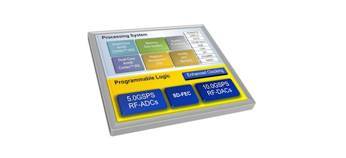
This hardware puts both the digital and analog domains into a single piece of silicon. While the digital side of the equation has benefitted from process node scaling, the analog side has not seen the same benefits, however Xilinx has put its hardware and software programmable engines, along with RF Analog technology, into 16nm TSMC hardware.
The RFSoC design is a single-chip adaptable radio platform. In previous generations, a system would rely on multiple chips to perform all the following tasks, but Xilinx has a solution it believes simplifies the design immensely. It integrates the RF signal chain, from MACs to DSPs, Radio IP, baseband, modulation, DSP signalling and filtering, and ADC/DAC, along with significant general purpose digital processors and a DDR4 memory subsystem.

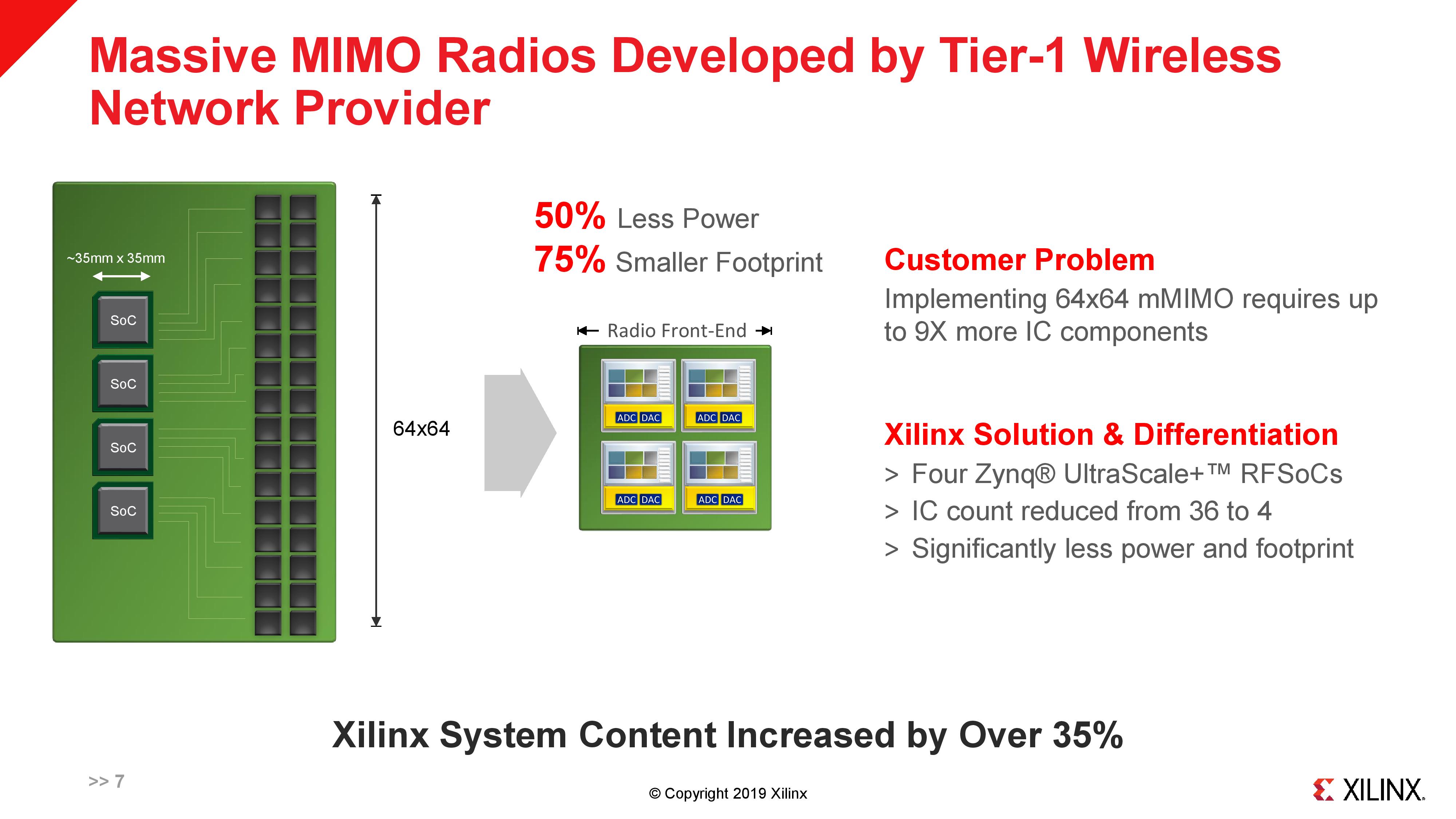
One of the benefits of the RFSoC, according to Xilinx, is in Massive-MIMO radios for wireless networks. According to the company, a 64x64 m-MIMO using RFSoCs reduces power consumption by half, makes the installation up to 75% smaller, and reduces the number of components in the system by 89%.

New Generation RFSoCs
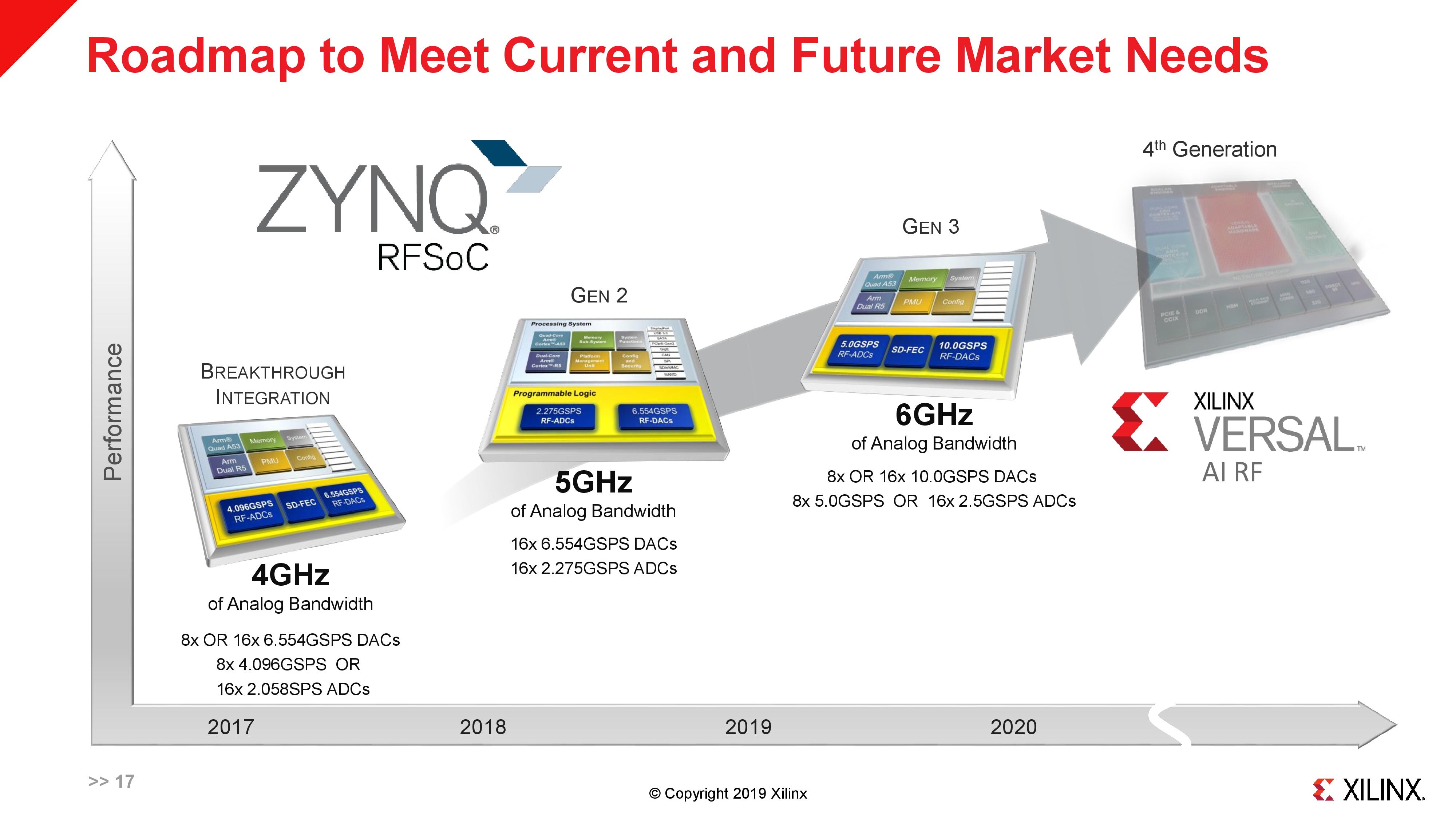
Today’s announcement is for the second generation and third generation of Xilinx’s RFSoC family.
The first generation covered bands up to 4 GHz and DOCSIS 3.1, enabling some positioning relative to 5G implementations. The second generation, which is a fast track tweak to the first generation for quick time to market, will cover up to 5 GHz, enabling the Chinese and Japanese markets to start deployments quickly. The third generation is an updated design which goes up to 6 GHz, enabling worldwide 5G deployments using both licenced and unlicensed spectrum.
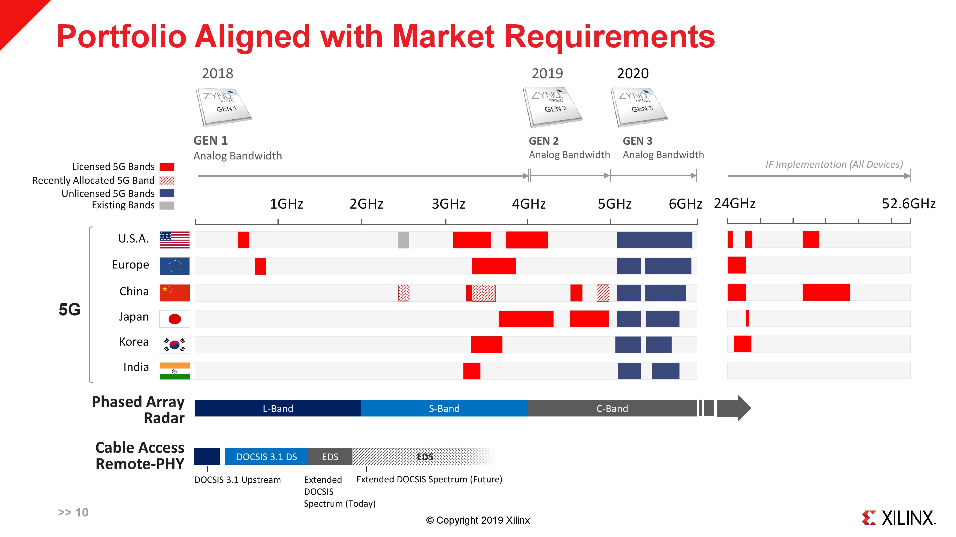
First out of the gate is the new second generation product. As mentioned, it is a tweaked enhanced version of the first gen for the Asian markets that want to start testing with their 5 GHz spectrum. Xilinx is stating that engineering samples are available for select customers now, with full production expected in June 2019.
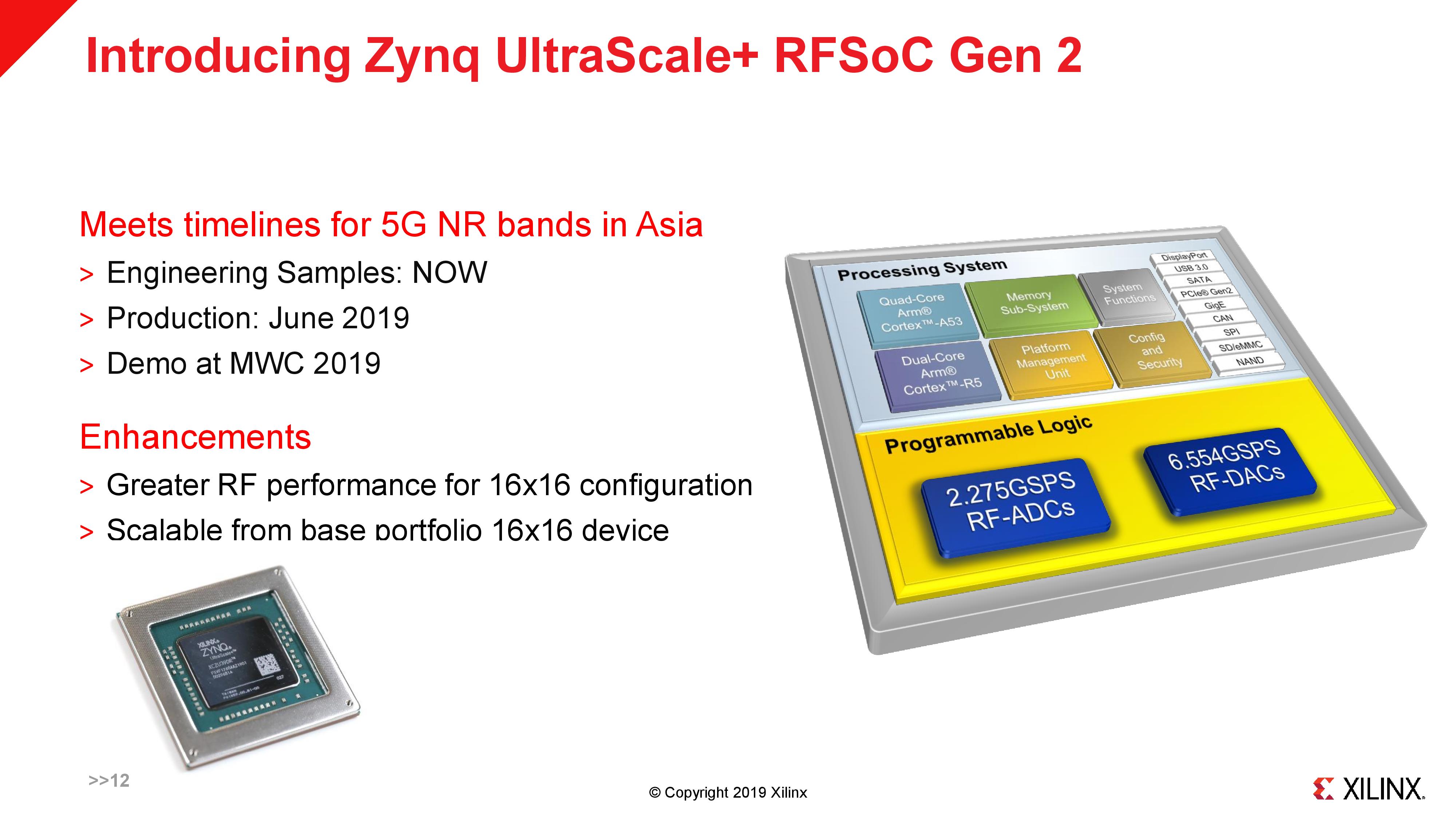
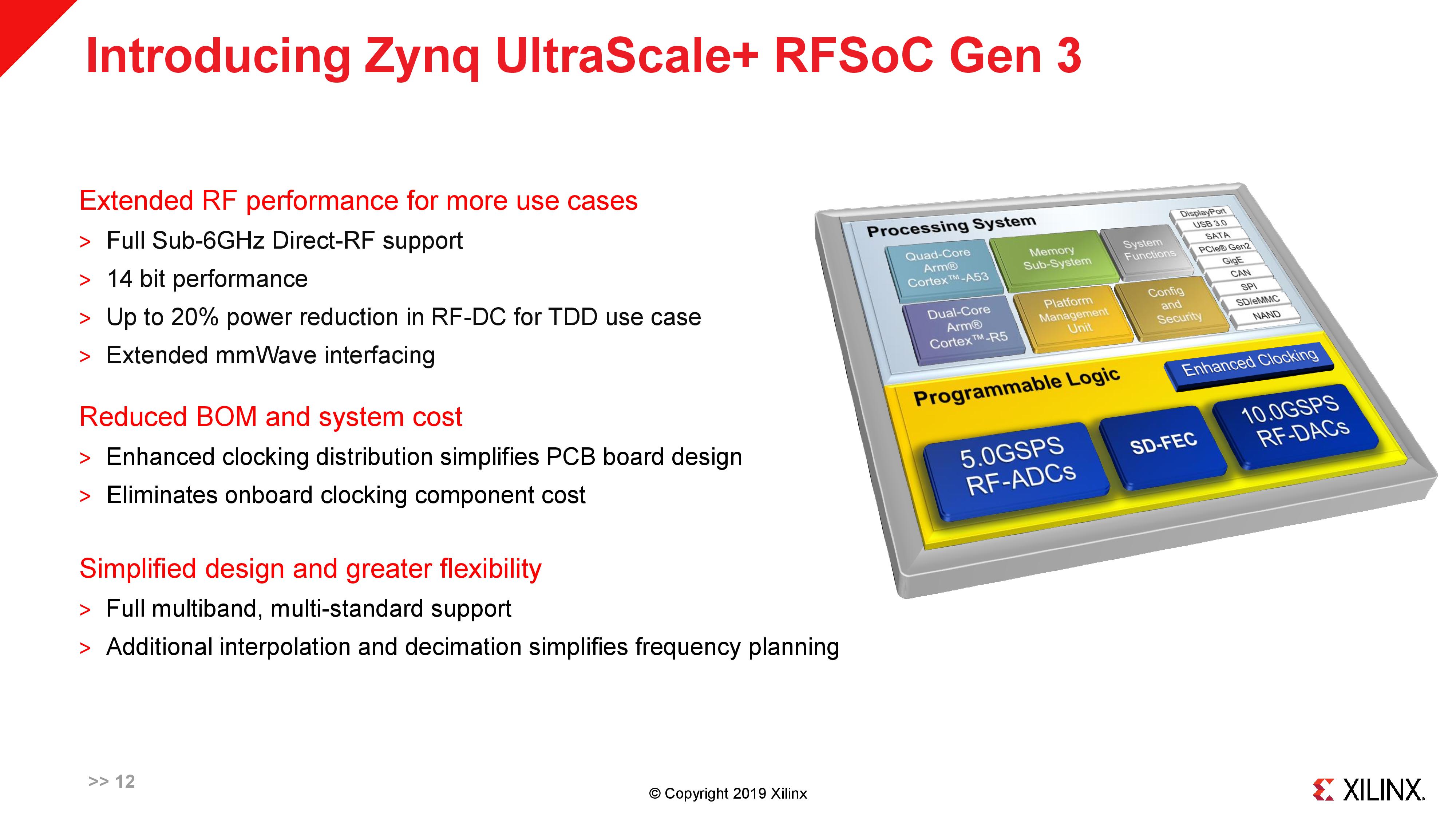
The third generation uses similar underlying hardware (quad-A53 and dual-A5 CPUs with programmable logic), but the fixed function ADC/DACs are upgraded and on a different clock domain to be able to support 6 GHz. This also enhances the clock of the programmable logic, especially for the additional DSP requirements of 6 GHz with up to 14-bit processing. Xilinx states that the third generation product will have a reduced power consumption on TDD, extended mmWave interfacing, and full multiband/multi-standard support. The enhanced clocking also means that in external clock generator mode, only one external clock generator is needed for the whole design, rather than up to four as previously required.
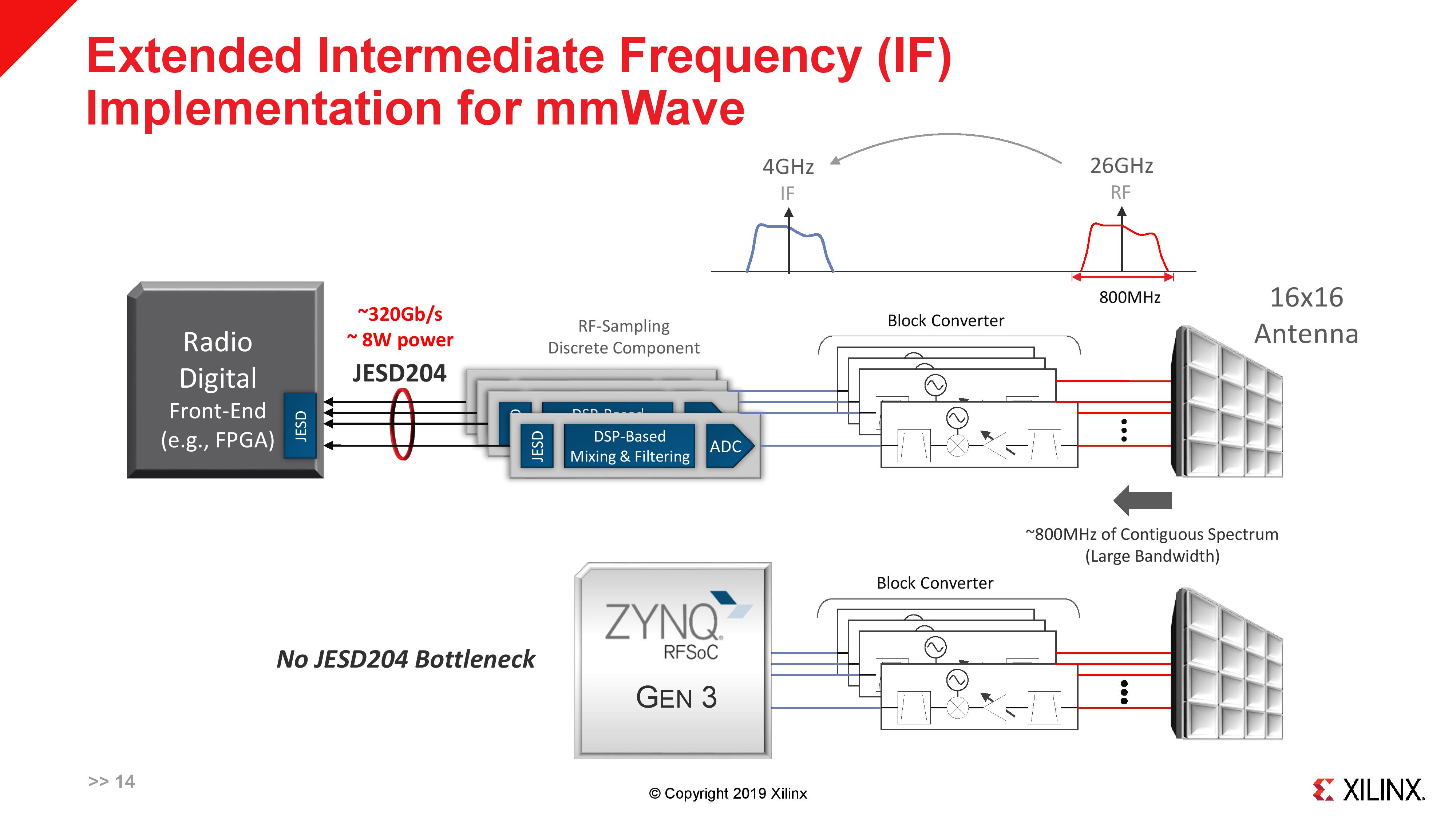
Xilinx states that its integrated analog/digital solution also helps with the extended intermediate frequency implementation for mmWave. One of the issues of traditional designs is that the interface between the RF-Sampling discrete DSPs and a digital front-end is a given standard, known as JESD204. When in a 16x16 antenna solution, this standard interface would consume about 8W at 320Gb/s, which is a lot of power when 800 MHz of high frequency spectrum needs to be analysed. By integrating the digital with the analog with the third generation components, that interface happens all inside the chip and can be proprietary, allowing for faster transmission at lower power.
With the design, Xilinx states that it allows tier-one vendors to use their custom programmable IP with the RF, while tier-two vendors can use their own or canned IP solutions. With the design, it enables Xilinx to add the RF market into its portfolio of products.
The third generation of RFSoC is sampling in the second half of 2019, with production in Q3 2020 (the timeline for testing and verification with vendors is longer than one might imagine), and the part will cover all the unlicenced sub-6GHz bands in one chip.
Both the second and third generation parts will be pin-compatible with the first generation hardware. Vendors interested in the new parts will have to speak to their local Xilinx representative for more information.
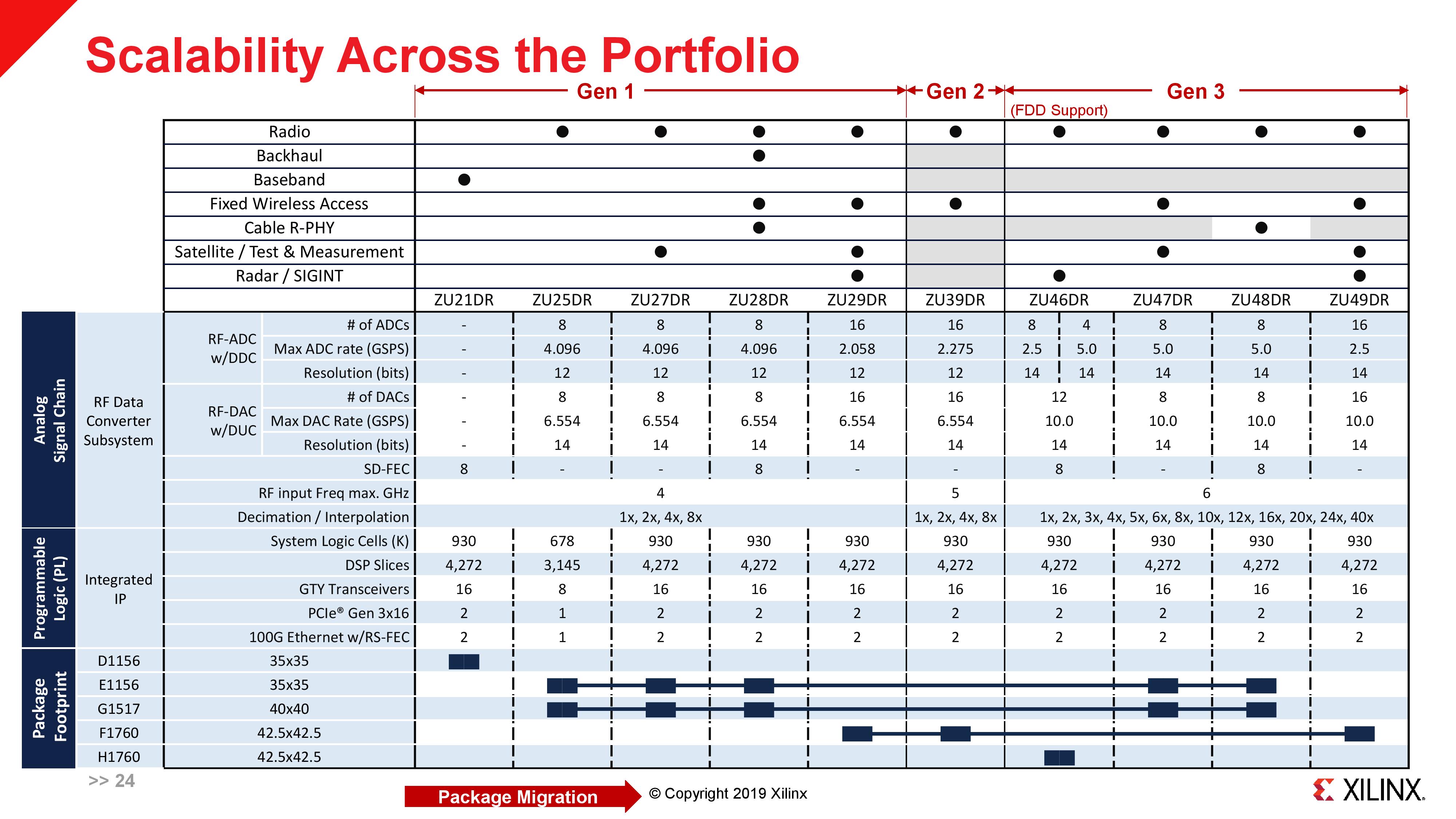
The product portfolio from Xilinx for Gen3 will mirror Gen1 for ADC and DAC units, albeit with higher rates. Gen2 is only a single part for that targeted Asian market.


6 Comments
View All Comments
ksec - Friday, February 22, 2019 - link
Thanks for posting this Ian. I know a lot of people aren't interested in this non-consumer type of news, but it is good to at least see some backend component vendor getting some spotlight. But we are still only at 64 Massive-MIMO? Which seems to be FDD Focused. I wonder how they were used in the TDD 128 x 128 Scenario.Ian Cutress - Friday, February 22, 2019 - link
I think that was just the example they gave. I was told the solution scales out very easily.nathanddrews - Friday, February 22, 2019 - link
Quick, someone let ATT know immediately: 6G has arrived!sharathc - Friday, February 22, 2019 - link
Yeah. #MAGAdougw03 - Sunday, February 24, 2019 - link
Can someone explain how this chip covers 6GHz BW with only 10GSps and 2.5GSps DAC/ADC? Are they doing some tricks with undersampling?IrwinFletcher - Wednesday, March 6, 2019 - link
The addressable bandwidth of the converters is 2-GHz according to their datasheets. They claim 4-GHz in their marketing buzz. 6-GHz is definitely marketing "enhancement". BTW at just a 2-GHz input signal, their effective resolution is maxed out at <9 bits which is really good, but hardly a 12b ADC or as they claim for Gen3 a 14b ADC. Funny thing is that being the only player in this game they don't need to lie in marketing campaigns, but they just can't resist temptation to tell a long tale.While this device is definitely a game changer for ADI (wake up Analog Devices!) they do need to figure out how to scale down 30W of power which is mostly due to 16nm FPGA technology. They should migrate this to 7nm or 5nm ASAP and get to their end game for power efficiency. After that it is a race to ASIC (harden FPGA logic) for power and cost reduction.