Synopsys to Accelerate Samsung’s 7nm Ramp with Yield Explorer Platform
by Anton Shilov on July 4, 2019 10:00 AM EST- Posted in
- Semiconductors
- 10nm
- 7nm
- Samsung Foundry
- 5nm
- 3nm
- 4nm
- Synopsys

Synopsys has announced an acceleration of development on its yield learning platform designed to speed up ramp up of chips made using Samsung Foundry’s 7LPP (7 nm low power plus) process and newser technologies. The Yield Explorer is a complex yield learning platform that is designed to analyze product layouts, fab data, and product test data in order to find weak spots and enable engineers to improve yields of various chips. Eventually, the Yield Explorer will be enhanced for Samsung’s 5 nm, 4 nm, and 3 nm nodes.
Production of modern chips is an extremely complex process that takes several months to accomplish and involves thousands of steps. Actual yields of chips depend on quality of their designs as well as their power and performance requirements. Therefore, to improve yields of a particular silicon chip, multiple things have to be analyzed to identify systematic yield limiters, and this is exactly what Synopsys’ Yield Explorer does.
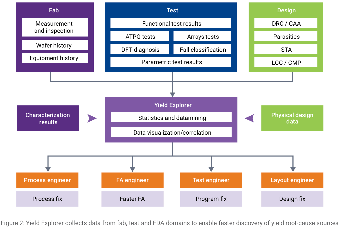
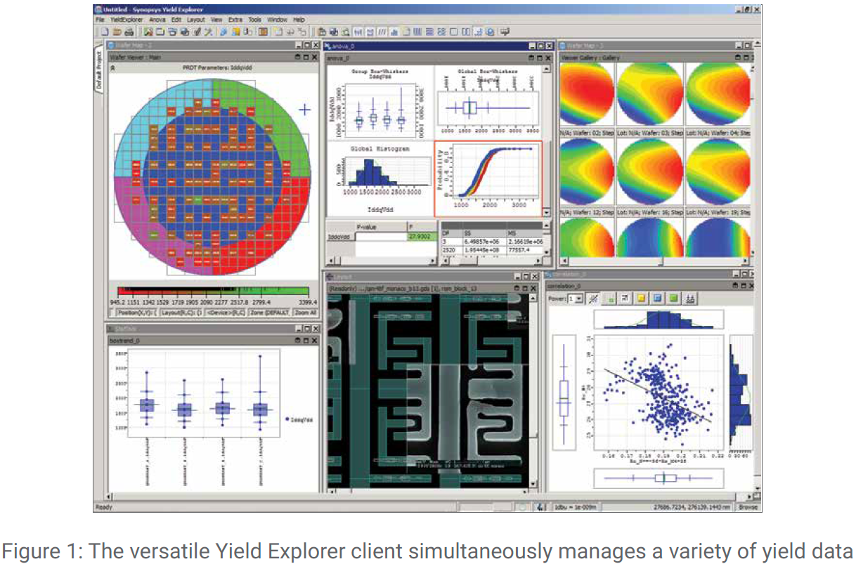
The Yield Explorer is a complex set of programs that analyzes data from three sources using advanced machine learning and data visualization techniques. First up, Yield Explorer analyzes product design, including layout and static timings. Secondly, the complex analyzes fab data, including inspection and metrology. Thirdly, the platform considers various product test data, such as binning, system level testing.
| Synopsys' Yield Explorer at a Glance | ||
| Source | Feature | |
| Product design data | Layout, netlist, test diagnosis, static timing analysis | |
| Fab data | Inspection, metrology, wafer acceptance test (WAT) | |
| Product test data | Bin, parametric, system-level test | |
Keeping in mind that silicon design is a property of the designer, whereas information about peculiarities of fab operations and characteristics is confidential, the platform that analyzes yields enables secure collaboration between the foundry and customer.
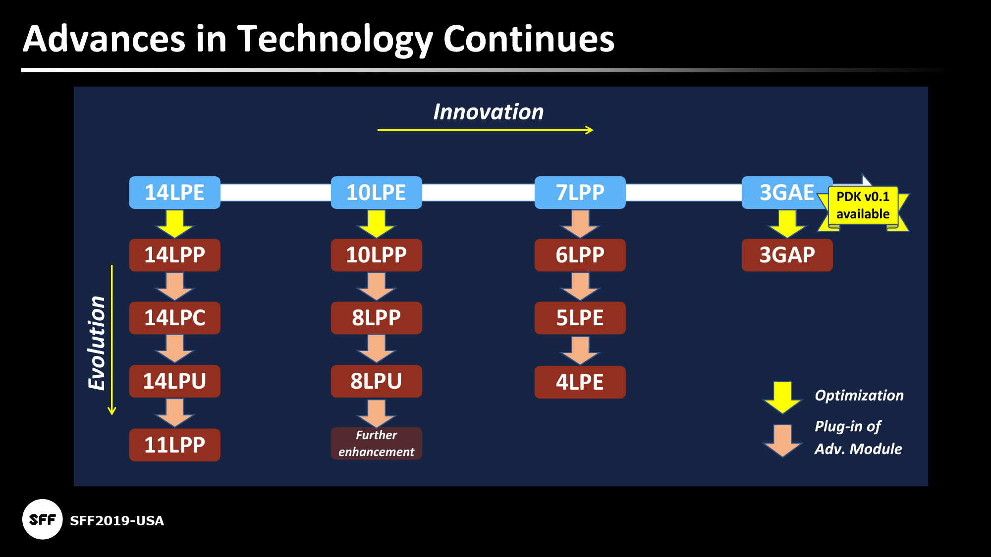
At present, Samsung Foundry and Synopsys offer Yield Explorer for designs produced using 10LPE, 10LPP, 8LPP, 8LPU, and 7LPP fabrication technologies (10 nm, 8 nm, and 7 nm nodes). Compatibility with 7LPP enables the two companies to leverage the platform to 5LPE, 4LPE (and possibly to 6LPP) processes. Furthermore, there is a plan to use Yield Explorer for chips made using 3GAE technology that uses gate all around MBCFET transistors based on silicon nanosheets.
"The secure collaboration model using Yield Explorer has greatly helped us to work efficiently with key customers to achieve target production yields quickly. We look forward to expanding this cooperation with Synopsys as we ramp up production on our 5-nanometer technology node."
- JY Choi, vice president of the Foundry Design Technology Team at Samsung Electronics
Related Reading:
- Samsung Starts Mass Production of Chips Using Its 7nm EUV Process Tech
- Samsung Completes Development of 5nm EUV Process Technology
- Samsung to Invest $115 Billion in Foundry & Chip Businesses by 2030
- Samsung Announces 3nm GAA MBCFET PDK, Version 0.1
Source: Synopsys


16 Comments
View All Comments
drexnx - Thursday, July 4, 2019 - link
I'm honestly surprised all of the pure-play foundries haven't been doing this for years, seems like a no-brainer?Hul8 - Thursday, July 4, 2019 - link
Apart from the ever increasing ML in computing in general, maybe they have, but the public just hasn't heard about it? Samsung's fab arm is pushing hard to expand their market share; Trying to convince customers about their advantages through a PR campaign like this would fit in that.Hul8 - Thursday, July 4, 2019 - link
Note that the technology is available for 10 nm and down, with no mention of when it was first introduced. This news item is about extending supporting to 7 nm:> Synopsys has announced an *acceleration of development* on its yield learning platform designed to speed up ramp up of chips made using Samsung Foundry’s 7LPP (7 nm low power plus) process and newser technologies."
(emphasis mine)
Samsung may have been using it since 10 nm first debuted. The reason to make so much noise about it now could (again according to my speculation) be because customers are unsure about Samsung's 7 nm.
Smell This - Friday, July 5, 2019 - link
Mmmm. Call me a skeptic but the *Yield Explorer* smells like the fanciful, ubiquitous (and dubious?) preemptive charts and graphs in the slide decks that proceeded the Chipzillah 14nm "Process-Architecture-Optimization (PAO)," or PAO+O+O+O.
"The secure collaboration model using Yield Explorer has greatly helped us to work efficiently with key customers to achieve target production yields quickly. We look forward to expanding this cooperation with Synopsys as we ramp up production on our 5-nanometer technology node."
Pretty much what *Hul8* said. I get that foundries want to optimize yields but bringing in 3rd-party 'consultants' can raise red flags.
zamroni - Friday, July 5, 2019 - link
software simulation really helps chip development because transistor is basically analog device and 0-1 transition is actually not rectangular with 0s delay in analog signalzamroni - Friday, July 5, 2019 - link
chip fabrication is very chemical and nanophysic thing. it's not simple 0 or 1. simulation software really helps to tune many aspects of the fabrication.Kevin G - Friday, July 5, 2019 - link
I do wonder if the amount of time this took to appear on the market is based upon how long it’d take to validate the results during development. The datasets for the design are huge even for a small chip. Then simulated results generated in development have to be compared to the reality of a production run and reconciled. With a wafer taking several months to make it through a factory, that’s a good chunk of time just waiting for results. Silver lining is that the simulation could have occurred concurrently with the production run since the chip designers were not leveraging this as part of their development workflow.With this software looking to be extended to smaller nodes, I would hope that Samsung and Synopsys are working with a customer who is going to be entering risk production on those nodes. Real production data will be invaluable for everyone else using these tools afterward.
Teckk - Thursday, July 4, 2019 - link
Every foundry l/IDM will have it some form and its details will be a pretty closely guarded piece of information. Yield will be the top priority especially with escalating costs as they try to go down towards lower nodes.Ray Chen - Thursday, July 4, 2019 - link
They have. Other foundries just don't use that "Yield Explorer" with a UI design from the 1990s.Death666Angel - Thursday, July 4, 2019 - link
Looks like every other solid lab program I've used. The "prettier" ones often have more bugs than these bare bones programs not designed to coddle the user.