TSMC Radically Boosts CapEx to Expand Production Capacities, To Reach $14B For 2019
by Anton Shilov on October 18, 2019 10:30 AM EST
Forecasting strong demand for its 5 nm and 7 nm class process technologies in the coming years, TSMC has announced that it's increasing its capital expenditure for 2019 by a whopping 36% - 40% over its earlier plans. The lion’s share of the additional money will be spent on the equipment that will be used to make 5 nm chips.
TSMC expected its 2019 CapEx to be between $10 billion and $11 billion early this year (in line with $10.5 billion in 2018), but increased demand for chips to be made using one of its 7 nm-class nodes (N7, N7P, N7+, N6) and projected demand for 5 nm semiconductors made the foundry change its mind. At its conference call with analysts and investors this week, TSMC said that it had decided to raise its 2019 CapEx by $4 billion to increase production capacities available to its customers. The company now expects its capital expenditure for the full year to be between $14 billion and $15 billion. Furthermore, TSMC upped its CapEx forecast for 2020 and expects it to be similar to the revised CapEx for this year.
According to TSMC, $1.5 billion of the $4 billion will be spent to increase its 7 nm capacity, whereas $2.5 billion will be used to increase 5 nm capacity. The company did not disclose what kind of equipment it intends to buy, but in the light of the fact that its 5 nm technology will heavily use extreme ultraviolet lithography (EUVL) on up to 14 layers, and the fact that both N7+ and N6 also use EUVL on up to four and five layers respectively, it is safe to say that some of the money will be spent on ASML’s latest Twinscan NXE step-and-scan systems.
From a chip designer’s perspective, TSMC’s N5 looks extremely attractive compared to N7, as it offers an up to 1.84x higher transistor density (i.e., enables to shrink die size of a given chip by up to ~45.6%), a 15% performance increase (at the same complexity and power) or an up to 20% power reduction (at the same frequency and complexity). TSMC’s N7+ also looks quite good (compared to N7) with its 1.15 – 1.20x higher transistor density and around 10% lower power consumption.
TSMC considers both 5 nm and 7 nm to be ‘long’ nodes, which means they will be used for years to come by tens of its customers, and is why it needs additional capacities to meet demand. Meanwhile, the first fabs to make chips using EUVL on multiple layers are already in place: TSMC’s Fab 15 is producing SoCs using N7+, whereas TSMC’s Fab 18 (the first phase of equipment move-in was completed in March 2019) is ready to start making commercial N5 chips sometimes in Q2 2020. Otherwise, it's important to note is that lead times of fab investments are on the scale of quarters; so while the money are formally spent in Q4, the actual production capacities will come online only sometimes in 2020.
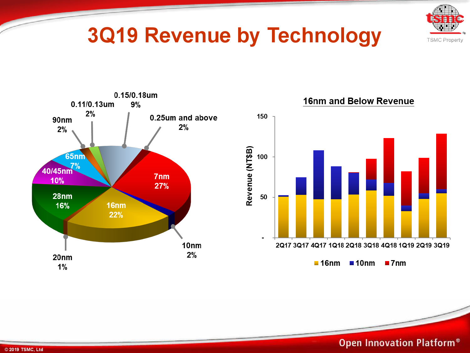
Demand for advanced process technologies (16 nm and below by TSMC’s definition) is very high in general these days. According to TSMC, SoCs for smartphones, HPC, and IoT applications accounted for a whopping 87% of its revenue in the third quarter. All of these SoCs these days demand a high transistor density, decent frequencies, and the lowest power consumption possible, which is why chip designers tend to use technologies with FinFET transistors and various enhancements that maximize performance, improve power savings, and/or increase transistor density (which allows customers to cut costs by making smaller chips or pack more features into a chip of a regular size and increase their value).

Advanced technologies accounted for a 51% of TSMC’s $9.4 billion wafer revenue in Q3 2019. From wafer revenue perspective, various 7 nm technologies brought TSMC 27% of its revenue last quarter, the highest share of all nodes. That said, it is not surprising that the company is increasing CapEx to meet demand for its leading-edge process technologies.
Here is what Wendell Huang, CFO of TSMC, had to say:
In TSMC, we build capacity according to our customer's demand. To forecast such demand, we take into consideration not only from each individual customer's indication, but also our own forecast based on macro as well as market segment outlook. Given the stronger outlook for 5G deployment next year, the demand for our 7-nanometer and 5-nanometer has increased significantly in the last few months.
We have, therefore, decided to raise our full year 2019 CapEx by USD 4 billion to meet this increased demand. We now expect our 2019 CapEx to be between USD 14 billion and USD 15 billion. About USD 1.5 billion of the USD 4 billion Capex increase is for 7-nanometer capacity and $2.5 billion is for 5-nanometer capacity.
Related Reading:
- TSMC Starts to Build Fab 18: 5 nm, Volume Production in Early 2020
- TSMC: N7+ EUV Process Technology in High Volume, 6nm (N6) Coming Soon
- TSMC: 3nm EUV Development Progress Going Well, Early Customers Engaged
- TSMC Announces Performance-Enhanced 7nm & 5nm Process Technologies
- TSMC Details 5 nm Process Tech: Aggressive Scaling, But Thin Power and Performance Gains
- TSMC: No Plans to Buy Rivals at The Moment
- Samsung to Invest $115 Billion in Foundry & Chip Businesses by 2030
Source: TSMC


18 Comments
View All Comments
PeachNCream - Friday, October 18, 2019 - link
Typo in "$10 billion and $11 bullion"psychobriggsy - Friday, October 18, 2019 - link
https://www.deviantart.com/kipine/art/Bull-Lion-70...prisonerX - Friday, October 18, 2019 - link
No, that's correct, they're paying for it in gold.neogodless - Friday, October 18, 2019 - link
HPC is an acronym for "high-performance computing" (and not my initial guess, which was Home/Personal Computers.)sartwell - Friday, October 18, 2019 - link
HPC = GPUabufrejoval - Friday, October 18, 2019 - link
IMHO that's too simplistic and temporary. HPC will also evolve into more distinct use cases and configurations while the benefits of game-GPU and GPGPU co-design will shrink.Dragonstongue - Friday, October 18, 2019 - link
pretty sure not, other had right, HPC = things like EPYC and such, however, something like Nvidia workstation class (not below) would quantify as HPC (if they ONLY for compute purpose) of which there are VERY few, otherwise would be GPU (general purpose unit - graphics (in all parts of course)^.^
brucethemoose - Friday, October 18, 2019 - link
Almost 10% of revenue comes from 0.15/0.18 micrometer nodes? They must be selling a ton of those, given how old and (relatively) cheap the node is... I wonder who's buying them?wrkingclass_hero - Friday, October 18, 2019 - link
Maybe it's used to manufacture image sensors? When Samsung released the nx-1 they said that their 32 nanometer image sensor was much smaller than the competition with Canon having 150 mm technology and Sony having about 300nm (or maybe vice versa.)prisonerX - Friday, October 18, 2019 - link
Those chips that don't need anything smaller.