Imagination Announces A-Series GPU Architecture: "Most Important Launch in 15 Years"
by Andrei Frumusanu on December 2, 2019 8:00 PM ESTFixed Function Changes & Scalability
Zooming out from the ALU, we’re seeing a higher-level block configuration that’s very similar to past Imagination PowerVR GPUs. The ALUs themselves are still housed in the larger cluster block that’s called the USC, or unified shading cluster. The USC along with various other fixed function blocks is in turn housed in an SPU, or shader processing unit, effectively the scaling block regularly referred to as a “core”.
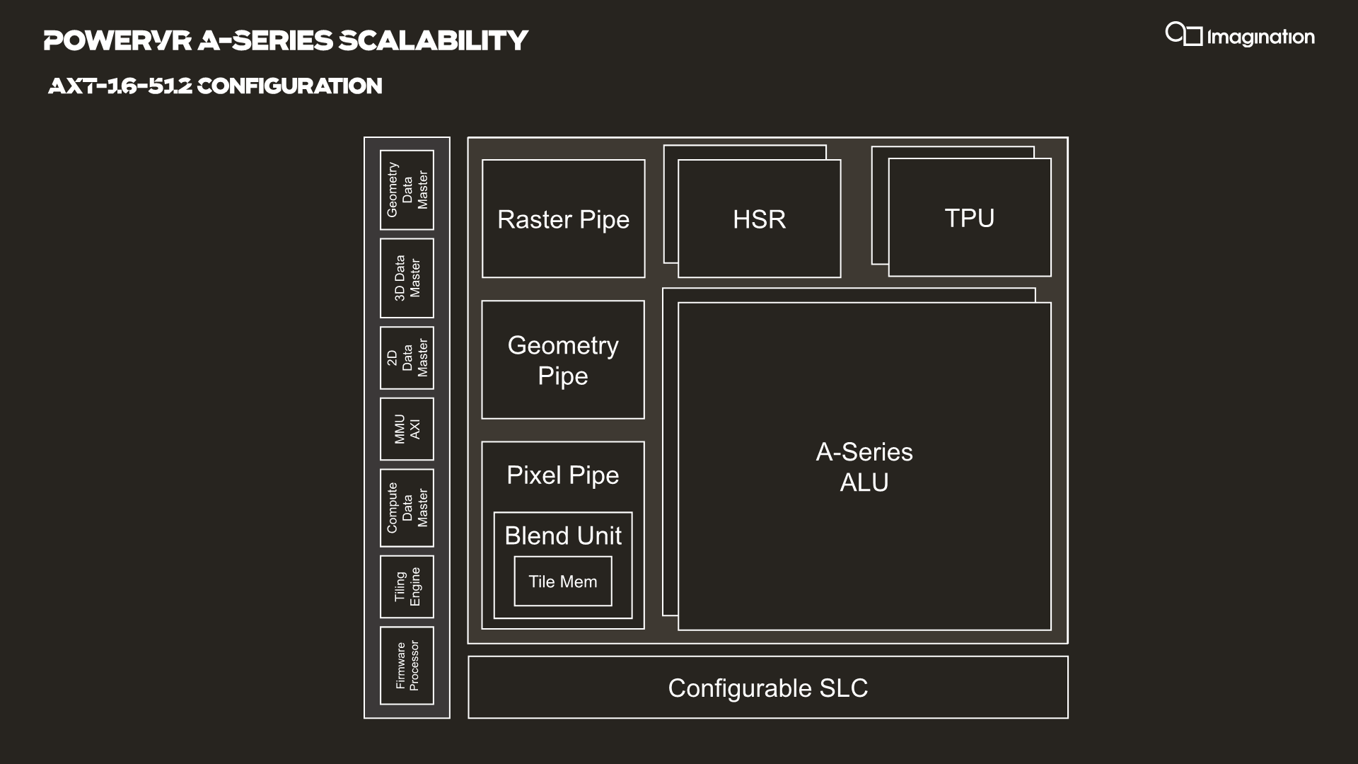
Each SPU houses two USCs in the current IP configuration, meaning we have two clusters of 128-wide ALUs. This is valid for all AXT parts, but we imagine the AXM-8-256 unit just has a single USC. The AXT-16-512 is the smallest configuration with a fully populated SPU.
Each SPU has its own geometry pipeline, and up to two texture processing units. The A-Series carries over the per-TPU throughput design from the Furian architecture, meaning the block is able to sample 8 bilinear filtered texels per clock. The A-Series doubles this up now per SPU and the AXT models feature two TPUs, bringing up the total texture fillrate to 16 samples per clock per SPU.
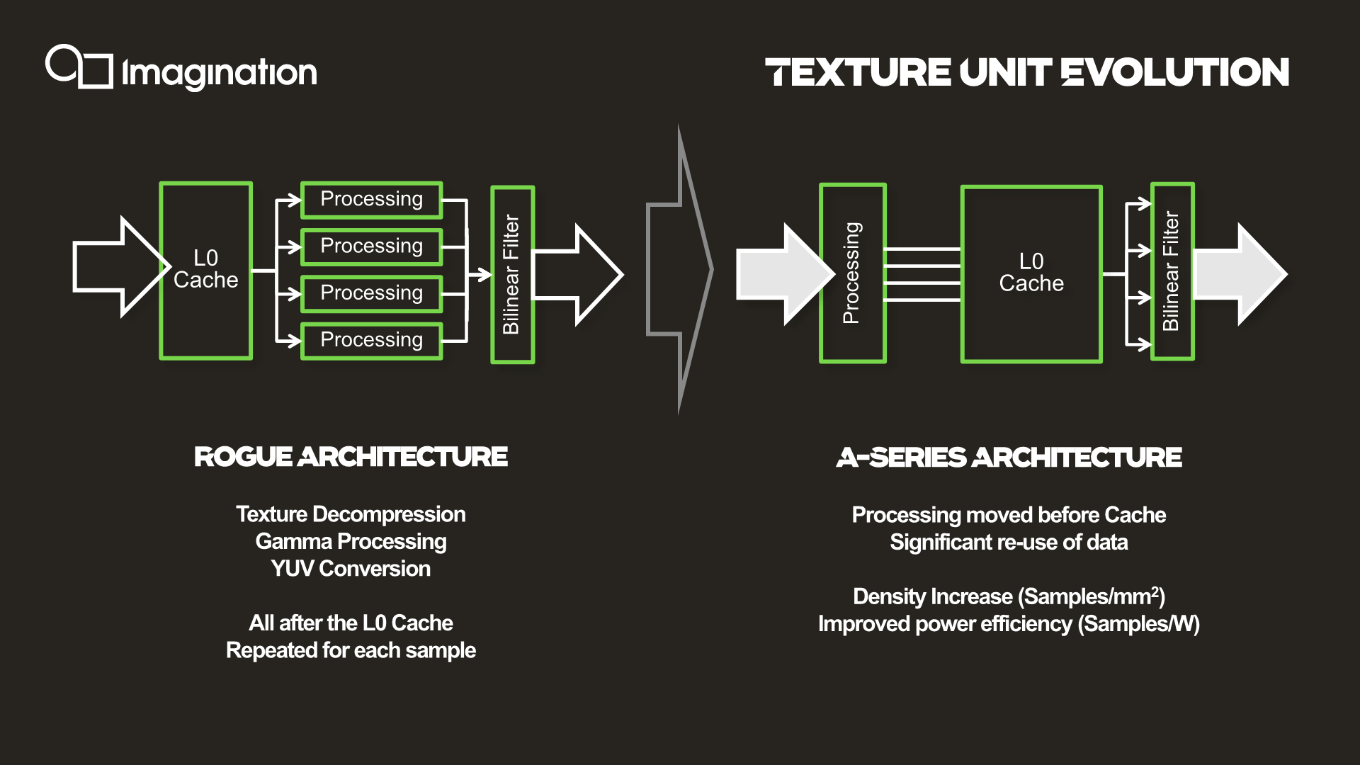
The microarchitecture of the texture units has also evolved beyond just their throughput. A bigger improvement that Imagination is disclosing is the handling and location of the L0 cache. The L0 cache has been relocated within the texturing workflow to between the processing and filtering stages, allowing the L0 cache to hold the outputs of the processing stage, rather than the inputs. This allows for what Imagination calls significant data reuse, as texels don't need to be re-processed each time they're needed. And given how many times a texel may need to be sampled during anisotropic filtering, it's easy to see why. With the benefit of hindsight, this seems like an obvious improvement to make, but the company says that the design choices of the legacy configuration made sense at the time of conception and the workloads back then.
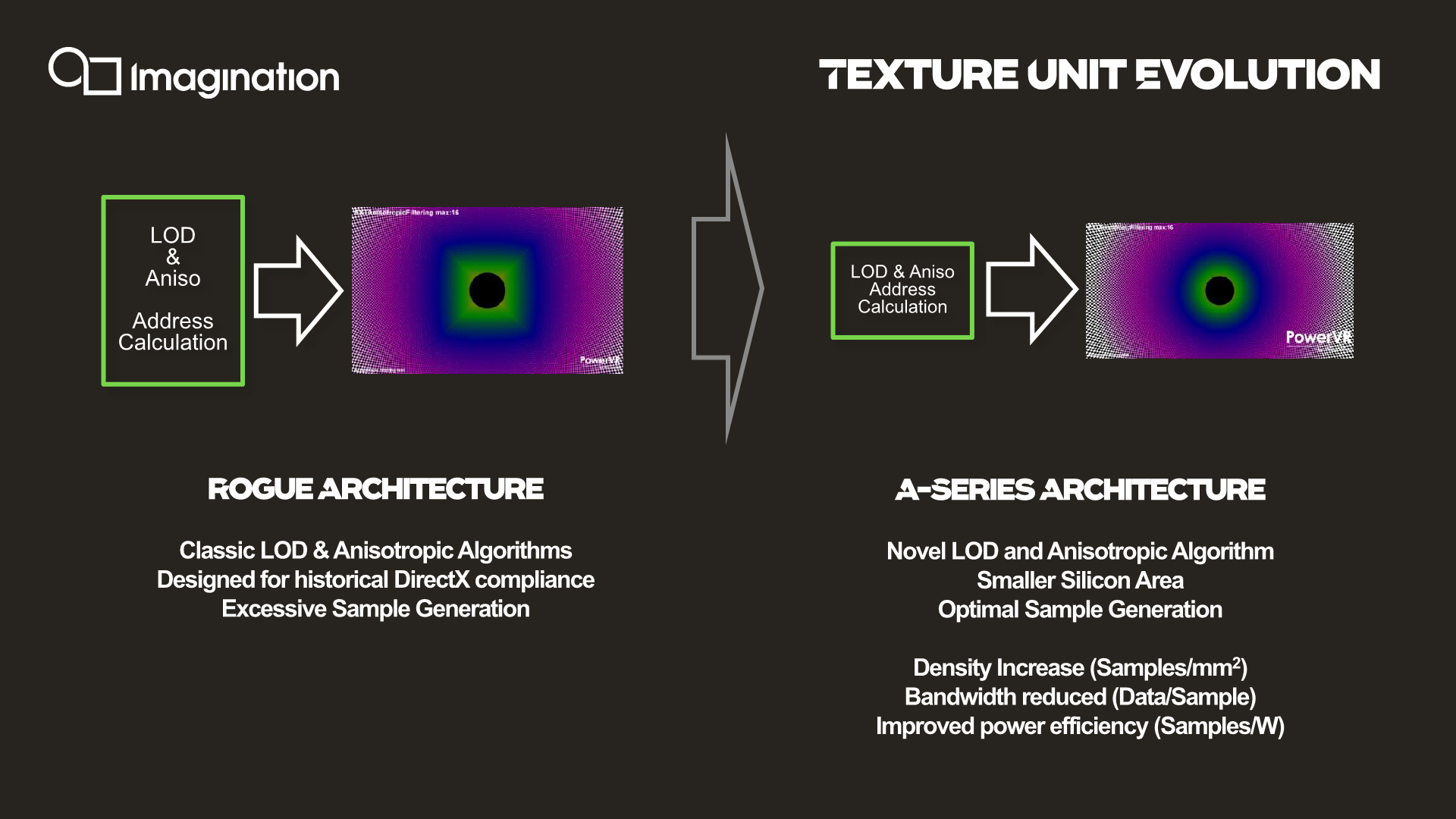
Imagination also talks about how the anisotropic filtering quality of the new architecture is much improved. In a set of comparison screenshots using a traditional texture tunnel, Imagination is showcasing that its new anisotropic filtering algorithms are far closer to being angle-independent – the ideal outcome for aniso filtering – as opposed to angle-dependent filtering with rather hard 90 degree angles on Rogue. Interestingly, Imagination is claiming that they've achieved this improved angle-independence even with fewer fewer samples, all of which serves to improve their efficiency and hardware density. With all of that said, since the comparison is against the Rogue architecture, I’m not entirely sure if it’s an actual novelty of the A-Series or rather a rehash of the anisotropic improvements that already got introduced in the 9XM series last year.
Another change in the fixed function units is found in the pixel pipeline, although superficially the throughput here doesn’t change compared to what we’ve seen on Furian. There’s still up to two PBEs with throughputs of up to 4 pixels per clock, and the design houses two such units for a total of 8 pixels per clock per SPU. There’s actually more internal distinction of the units though – at the front and back core it’s still able to handle 16 pixels per clock and also blend at 16 pixels per clock, although it’s limited on write out to 8 PPC on 1:1 pixel:texture situations.
Imagination’s doubling of the texture throughput whilst maintaining a steady pixel throughput means that the company is generally matching the decreasing pixel:texel fillrate throughput ratio we’ve also seen in other architectures such as from Qualcomm as well as the new Mali-G77, and now falls in at a 1:2 pixel:texel for the A-series.
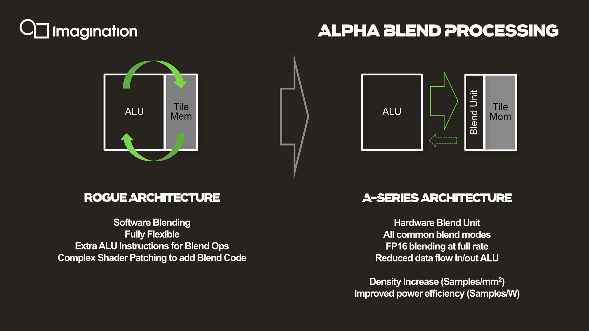
Alpha blending is now done on a dedicated hardware unit in the pixel pipeline instead of being computed by the ALUs. The change results in higher performance through the use of fixed function hardware, allowing for things such as FP16 blending at full rate, and frees up the ALUs themselves so that they can use their computation resources on other work. Density is improved, but more importantly it’s also improving power efficiency as it’s avoiding using more expensive and less task-specific hardware for the same tasks.
It’s to be noted that for the AXM series, the company uses customized fixed function units that are more area efficient, rather than just only scaling the numbers of units.
Scaling Things Up
With the SPU being the coarsest scaling block of the architecture, Imagination is building larger GPU configurations by simply adding in more SPUs. Essentially this is the “core” scaling of Imagination's GPU designs.
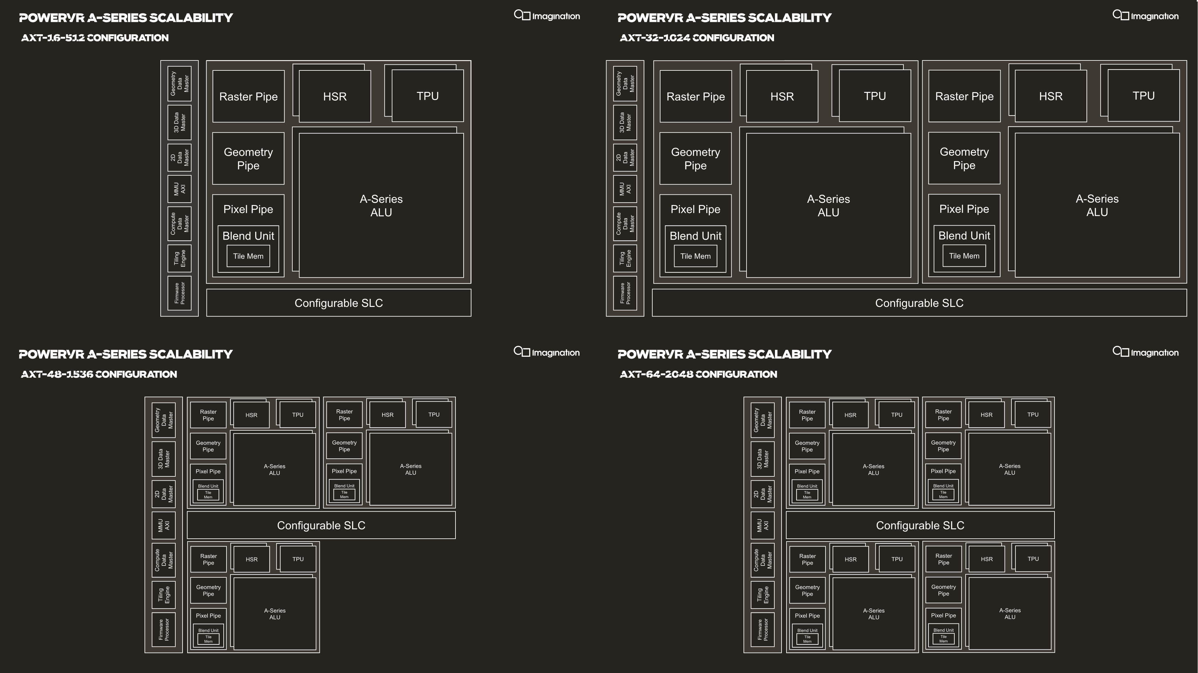
Scaling of SPUs across the AXT line happens in multiples of 16-512 across the range, both in terms of their product names as well as their texture and FLOPs/clock capabilities, which is rather simple to grasp and very quickly understand a configuration’s capabilities. As mentioned in the introduction, Imagination views the AXT-32-1024 as being the most popular choice for vendors targeting the high-end premium smartphone SoC segment, which possibly some vendors opting to go with the AXT-48-1536 for a larger area and lower clock speeds for more efficiency. The AXT-64-2048 would be a really big GPU which the company could build if there’s costumer interest.
| PowerVR GPU Comparison | ||||
| AXT-16-512 | GT9524 | GT8525 | GT7200 Plus | |
| Core Configuration |
1 SPU (Shader Processing Unit) - "GPU Core" 2 USCs (Unified Shading Clusters) - ALU Clusters |
|||
| FP32 FLOPS/Clock MADD = 2 FLOPs MUL = 1 FLOP |
512 (2x (128x MADD)) |
240 (2x (40x MADD+MUL)) |
192 (2x (32x MADD+MUL)) |
128 (2x (16x MADD+MADD)) |
| FP16 Ratio | 2:1 (Vec2) | |||
| Pixels / Clock | 8 | 4 | ||
| Texels / Clock | 16 | 8 | 4 | |
| Architecture | A-Series (Albiorix) |
Series-9XTP (Furian) |
Series-8XT (Furian) |
Series-7XT (Rogue) |
Comparing the smallest AXT-16-512 configuration with a single SPU and two USCs against similar configurations across the generations, we indeed see that the new A-Series does bring large architectural changes.
Imagination is marketing a 4x increase in ALU throughput, but again that’s against the 9XM GPUs, which are equal in ALU configuration to the Series-7XT in the table. However, it’s not to say that the increases aren’t any less impressive when comparing to the previous 9XTP family; a rise from 240 FLOPs/clock to 512 is still a 2.13x increase.
I think what’s actually more important to note here is the architecture has very big building blocks. At 512 FLOPs and 8 pixels per clock, an AXT SPU is significantly bigger than an Arm Mali-G77 core which comes in at “only” 64 FLOPs/clock and 2 pixels per clock, meaning an AXT core is roughly equivalent to eight G77 cores in computational power and four G77s in fillrate throughput, which is a massive difference in terms of design scaling. Naturally, in terms of effective density and power efficiency, few big cores will always win over a flock of small cores, as demonstrated by Qualcomm and Apple’s recent 2- and 4-core designs.


143 Comments
View All Comments
extide - Monday, December 2, 2019 - link
Not exactly an announcement I was expecting to see, but quite interesting. A bit ballsy, but that's pretty much what they need right now. We'll see how it shapes up in actual products...Kishoreshack - Monday, December 2, 2019 - link
This if's & but's in the industry is soo irritatingif it releases on time it will compete well
according to its release schedule we might be at the ending cycle of Mali G77 & introduction of G78
So the performance gains are almost negligible
Pessimist9 - Wednesday, December 4, 2019 - link
But they said it! Quick! Everyone to their brokers STAT!Kishoreshack - Monday, December 2, 2019 - link
Companies overpromising & under delivering is normCOUGH *INTEL*
Seriously until the GPU hits the market
I'm seriously not interested in speculation
I'm over speculation need result's to even be excited about this
Until it is implemented in real world
the idea remains a big cloud of doubt
Cause many companies fail to stick to their release schedule
eek2121 - Tuesday, December 3, 2019 - link
Intel has real GPU products currently, they are just integrated with Intel CPUs. I definitely wouldn't say Intel is 'behind schedule' with Xe either. If you read between the lines, they are shipping 7nm products in 2021, and one of these products is a high performance GPU. As a matter of fact, despite what Intel would have you believe, I suspect that they'll keep their 10nm launches to a minimum and jump straight to 7nm. It also would not surprise me if there is a shake-up in Intel's future that causes their fab business to get spun off into it's own entity to ensure that stuff like this doesn't happen again. That last part is pure speculation though.I'd be rather curious to see how an Intel/AMD/Nvidia GPU stacks up against the Imagination one.
Also note that apparently they aren't shipping open source drivers, which right away is going to create issues for them. NVIDIA is one of the few companies that chose this route, and thus far it's caused nothing but problems for both NVIDIA and the community at large.
Korguz - Tuesday, December 3, 2019 - link
" they are shipping 7nm products in 2021, " yea right,, ill believe that, when it actually happens.." causes their fab business to get spun off into it's own entity" i doubt that would happen. 10nm is VERY late, because they tried to do to much at once, or there is another reason, who knows.. but to spin it off??? not likely
regsEx - Tuesday, December 3, 2019 - link
10 nm is DUV process of highest ever density. It's denser than TSMC 7FF DUV. 7 nm, which is generation of TSMC N3, is EUV. It's easier.TheinsanegamerN - Tuesday, December 3, 2019 - link
That's why they are now 4 years behind schedule, right?mode_13h - Wednesday, December 4, 2019 - link
Exactly.I wonder which hurt Intel more: their over-ambitious process engineers or their greedy management. Either way, while they were sputtering and cavitating, the competition blew right by them.
Their once-unassailable lead was outmatched by their own hubris.
Santoval - Tuesday, December 3, 2019 - link
Intel's 7nm node is apparently going to be slightly denser than TSMC's 5nm node (N5), *not* their 3nm node (N3). I have read about numbers in the range of ~185 million transistors (MTr) per mm^2 for TSMC's N5 and ~200 MTr/mm^2 for Intel's 7nm node. TSMC's N3, in turn, will be 255+ MTr/mm^2. Beside a quite higher density TSMC will switch to GAA-FETs at 3nm, so there can be no direct comparison anyway. In any case Intel will need to deliver 7nm first, and I strongly doubt they will manage to completely master EUV manufacturing of multiple layers by 2021.By the way, Intel's 10nm is not denser than TSMC's N7 DUV. Intel has developed three 10nm variants, for low, mid and high density. Only the high density (and highest performance) 10nm variant is slightly denser than TSMC's N7 DUV and even that was already outclassed in density by TSMC's N7 EUV (7nm+).
To my knowledge Intel employs the mid density 10nm variant for the mobile Ice Lake parts they just released, so they haven't released and aren't about to release any 10nm SoC, CPU or GPU that is denser than even TSMC's vanilla (DUV) N7. Their sole high density (100+ MTr/mm^2) 10nm parts are probably their newest Agilex FPGAs.