Imagination Announces A-Series GPU Architecture: "Most Important Launch in 15 Years"
by Andrei Frumusanu on December 2, 2019 8:00 PM ESTHyperLane Technology
Another new addition to the A-Series GPU is Imagination's “HyperLane” technology, which promises to vastly expand the flexibility of the architecture in terms of multi-tasking as well as security. Imagination GPUs have had virtualization abilities for some time now, and this had given them an advantage in focus areas such as automotive designs.
The new HyperLane technology is said to be an extension to virtualization, going beyond it in terms of separation of tasks executed by a single GPU.
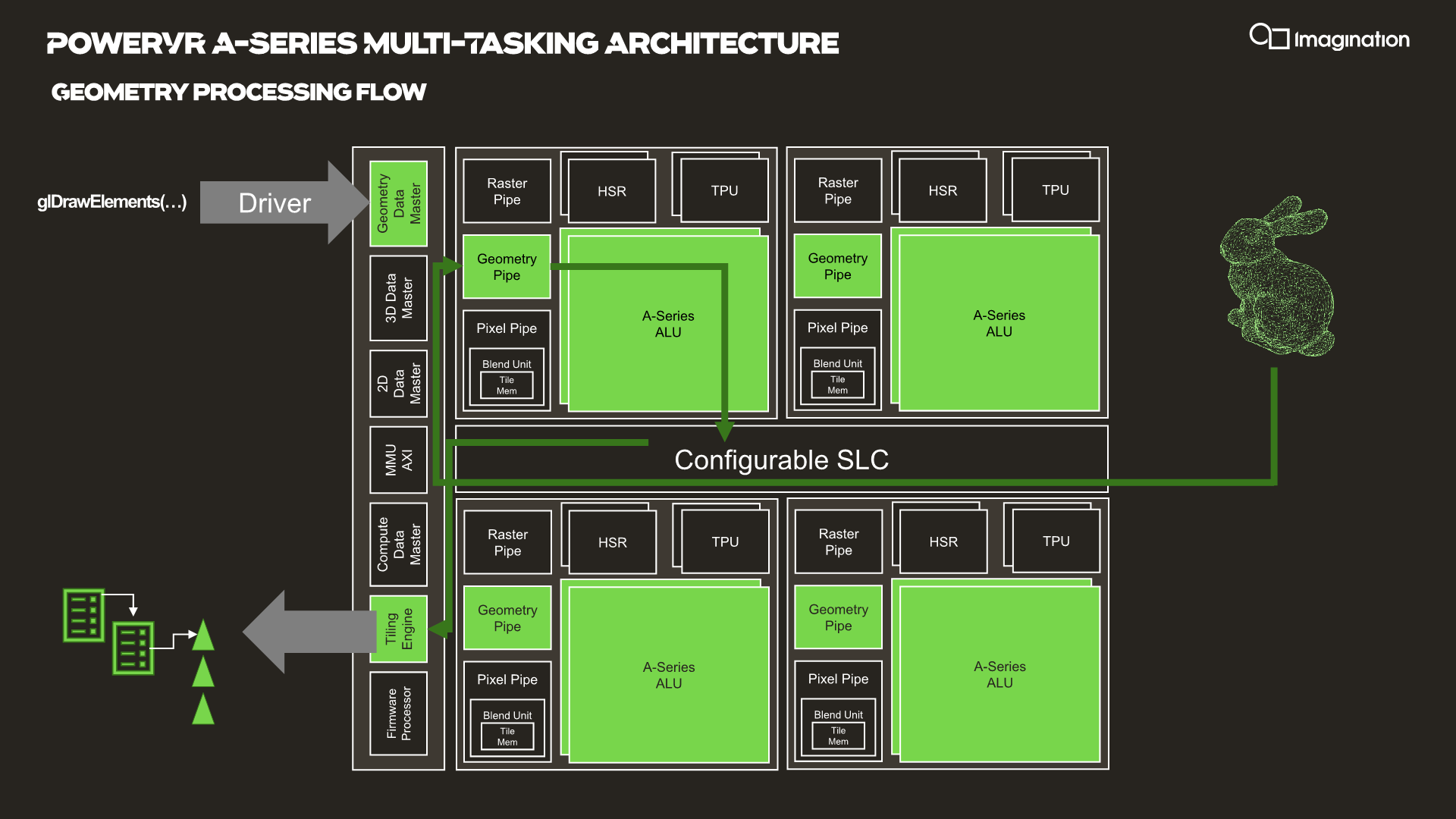
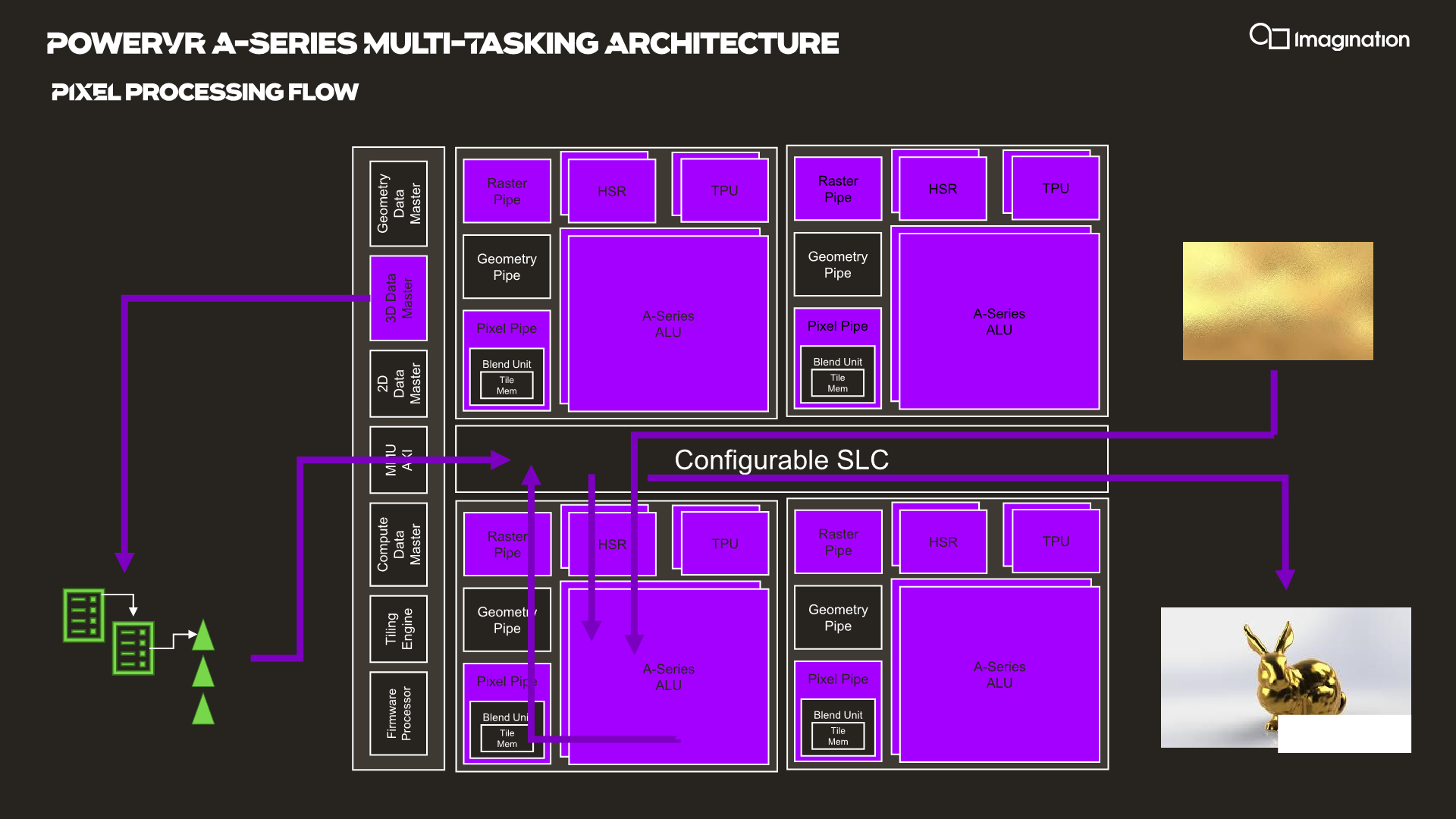
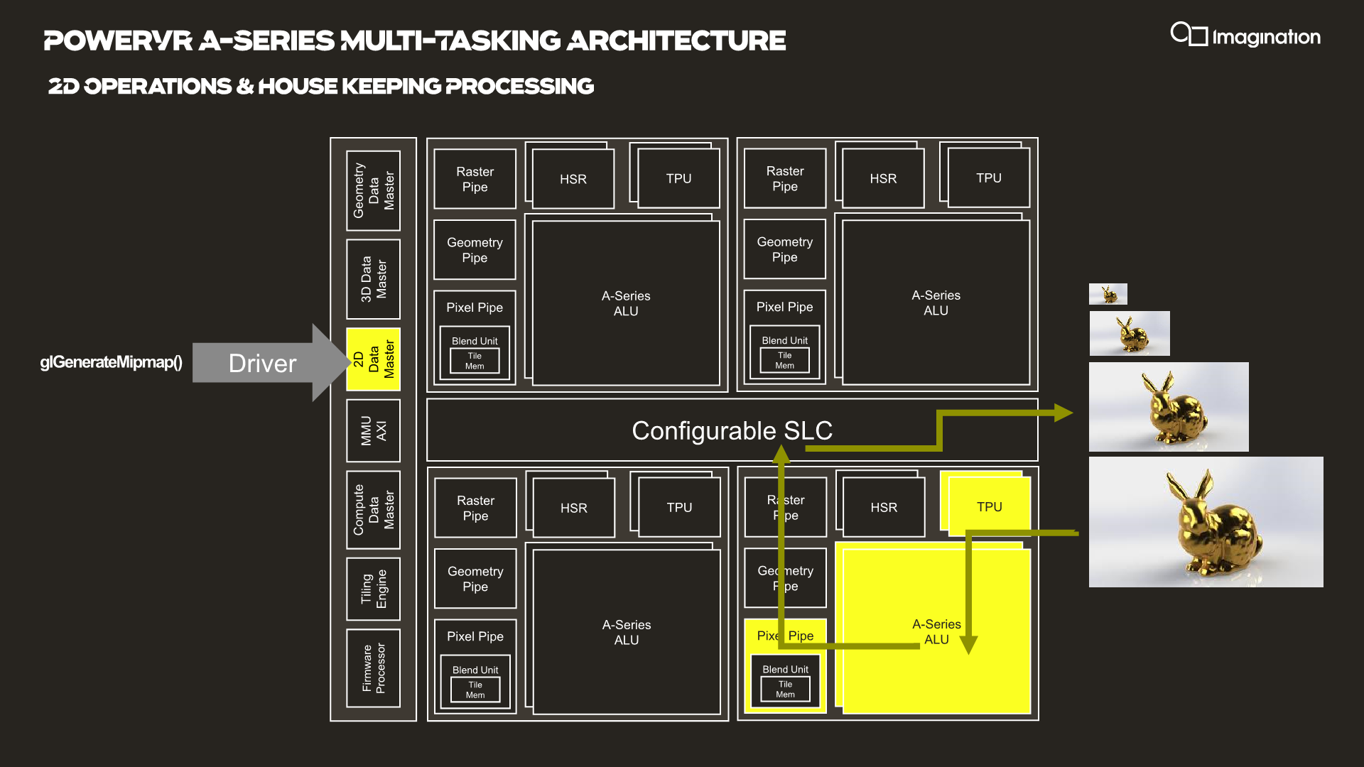
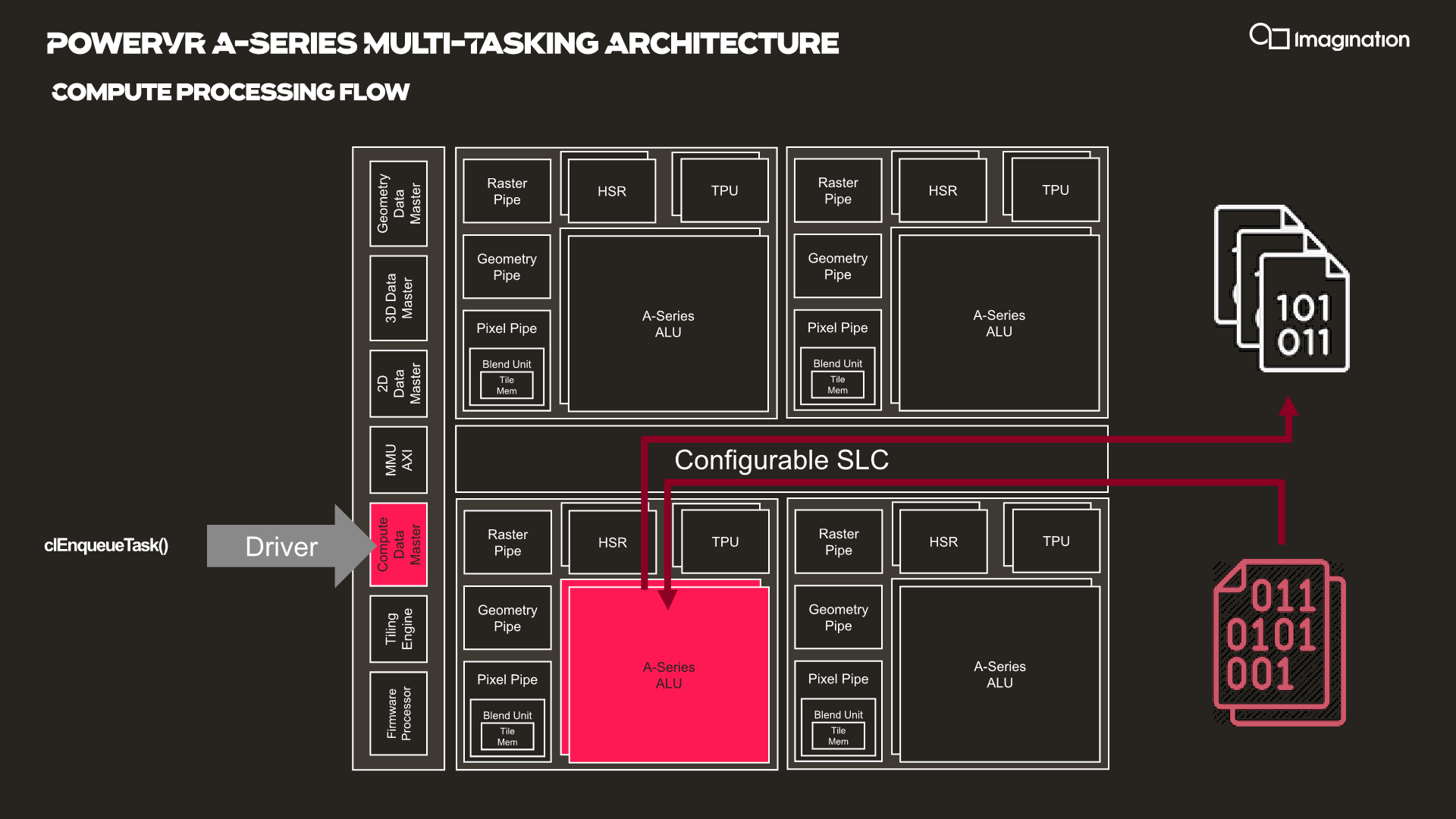
In your usual rendering flows, there are different kinds of “master” controllers each handling the dispatching of workloads to the GPU; geometry is handled by the geometry data master, pixel processing and shading by the 3D data master, 2D operations are handled by the 2D data, master, and compute workloads are processed by the, you guessed it, the compute data master.
In each of these processing flows various blocks of the GPU are active for a given task, while other blocks remain idle.
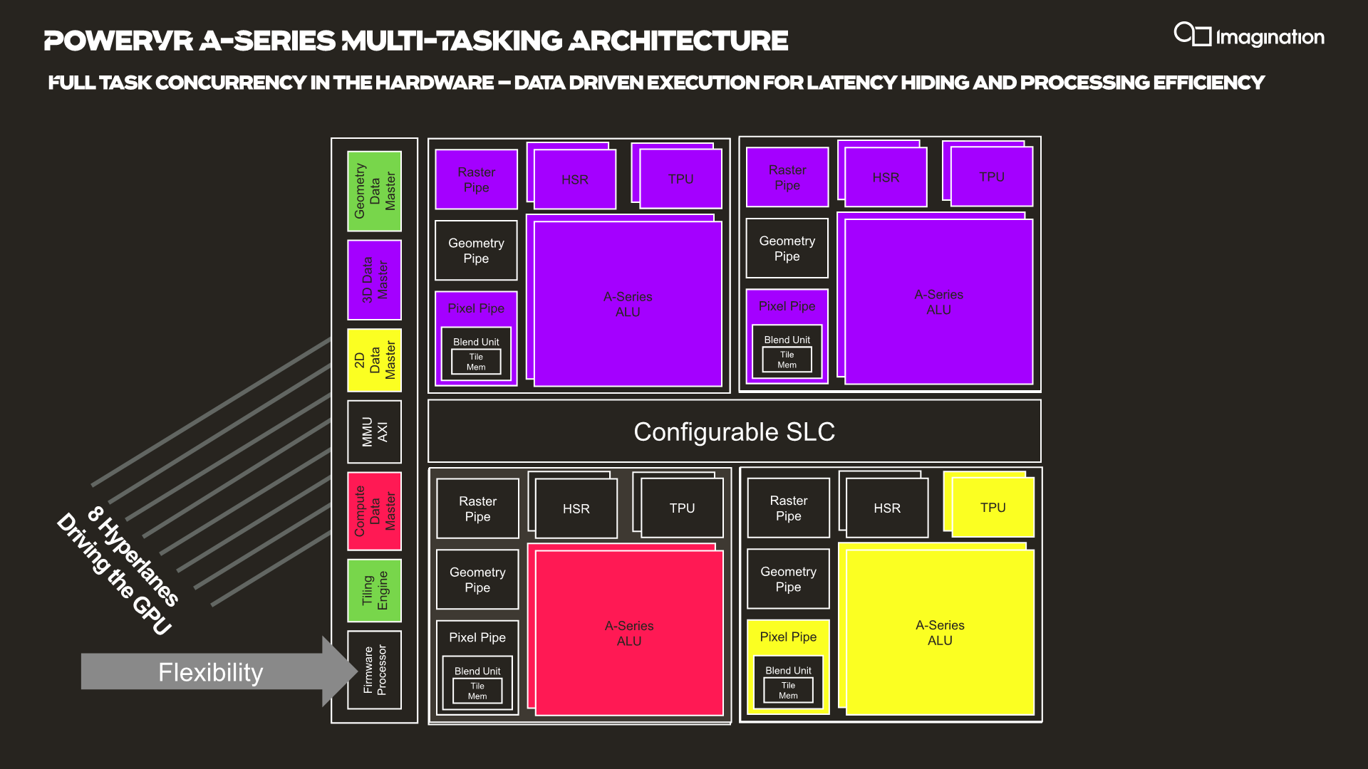
HyperLane technology is said to be able to enable full task concurrency of the GPU hardware, with multiple data masters being able to be active simultaneously, executing work dynamically across the GPU’s hardware resources. In essence, the whole GPU becomes multi-tasking capable, receiving different task submissions from up to 8 sources (hence 8 HyperLanes).
The new feature sounded to me like a hardware based scheduler for task submissions, although when I brought up this description the Imagination spokespeople were rather dismissive of the simplification, saying that HyperLanes go far deeper into the hardware architecture, with for example each HyperLane having being able to be configured with its own virtual memory space (or also sharing arbitrary memory spaces across hyperlanes).
Splitting GPU resources can happens on a block-level concurrently with other tasks, or also be shared in the time-domain with time-slices between HyperLanes. Priority can be given to HyperLanes, such as prioritizing graphics over a possible background AI task using the remaining free resources.
The security advantages of such a technology also seem advanced, with the company use-cases such as isolation for protected content and rights management.
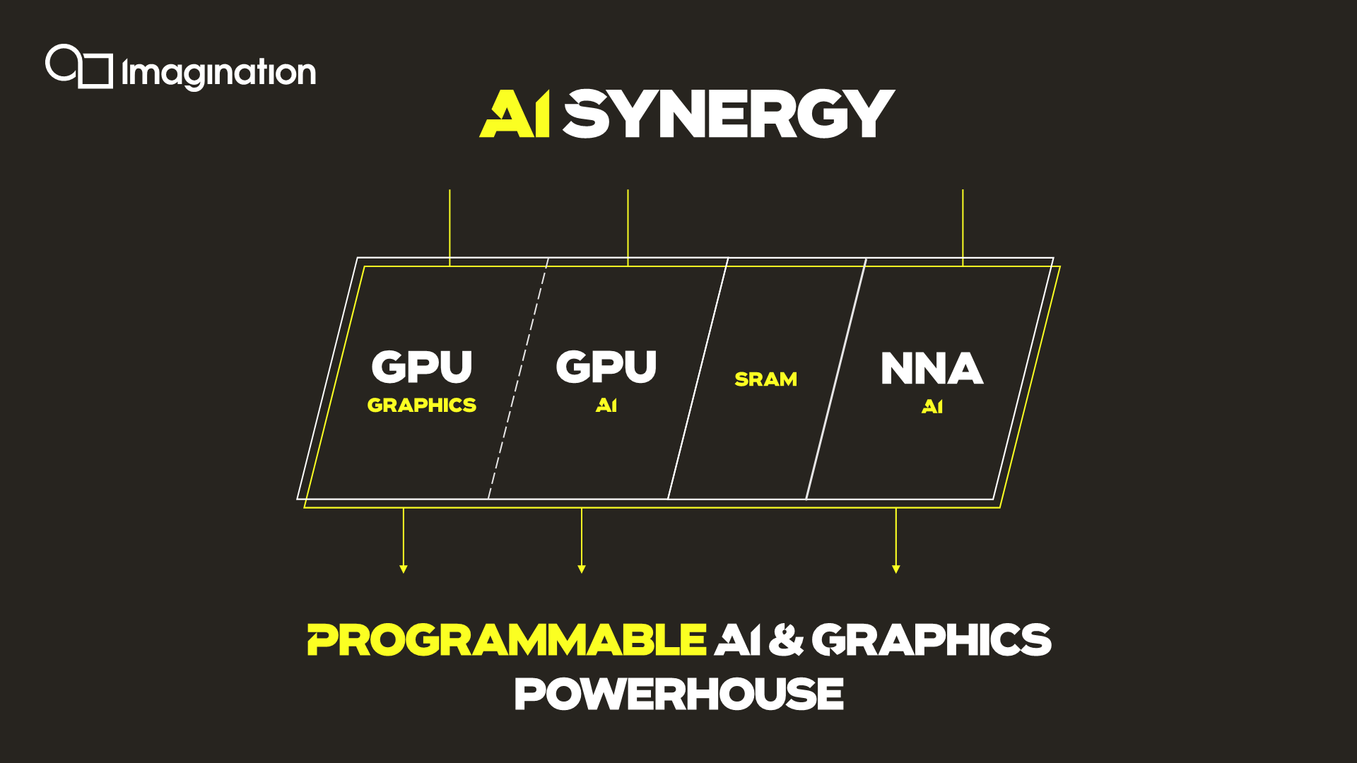
An interesting application of the technology is the synergy it allows between an A-Series GPU and the company’s in-house neural network accelerator IP. It would be able to share AI workloads between the two IP blocks, with the GPU for example handling the more programmable layers of a model while still taking advantage of the NNA’s efficiency for the fixed function fully connected layer processing.
Three Dozen Other Microarchitectural Improvements
The A-Series comes with other numerous microarchitectural advancements that are said to be advantageous to the GPU IP.

One such existing feature is the integration of a small dedicated CPU (which we understand to be RISC-V based) acting as a firmware processor, handling GPU management tasks that in other architectures might be still be handled by drivers on the host system CPU. The firmware processor approach is said to achieve more performant and efficient handling of various housekeeping tasks such as debugging, data logging, GPIO handling and even DVFS algorithms. In contrast as an example, DVFS for Arm Mali GPUs for example is still handled by the kernel GPU driver on the host CPUs.
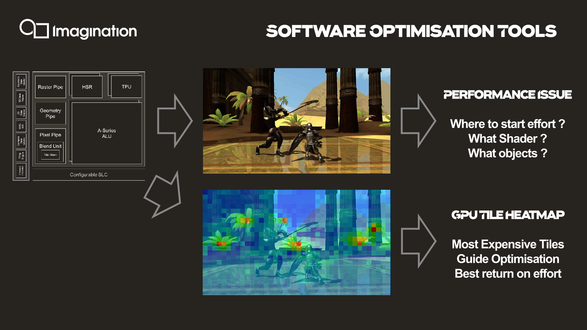
An interesting new development feature that is enabled by profiling the GPU’s hardware counters through the firmware processor is creating tile heatmaps of execution resources used. This seems relatively banal, but isn’t something that’s readily available for software developers and could be extremely useful in terms of quick debugging and optimizations of 3D workloads thanks to a more visual approach.


143 Comments
View All Comments
extide - Monday, December 2, 2019 - link
Not exactly an announcement I was expecting to see, but quite interesting. A bit ballsy, but that's pretty much what they need right now. We'll see how it shapes up in actual products...Kishoreshack - Monday, December 2, 2019 - link
This if's & but's in the industry is soo irritatingif it releases on time it will compete well
according to its release schedule we might be at the ending cycle of Mali G77 & introduction of G78
So the performance gains are almost negligible
Pessimist9 - Wednesday, December 4, 2019 - link
But they said it! Quick! Everyone to their brokers STAT!Kishoreshack - Monday, December 2, 2019 - link
Companies overpromising & under delivering is normCOUGH *INTEL*
Seriously until the GPU hits the market
I'm seriously not interested in speculation
I'm over speculation need result's to even be excited about this
Until it is implemented in real world
the idea remains a big cloud of doubt
Cause many companies fail to stick to their release schedule
eek2121 - Tuesday, December 3, 2019 - link
Intel has real GPU products currently, they are just integrated with Intel CPUs. I definitely wouldn't say Intel is 'behind schedule' with Xe either. If you read between the lines, they are shipping 7nm products in 2021, and one of these products is a high performance GPU. As a matter of fact, despite what Intel would have you believe, I suspect that they'll keep their 10nm launches to a minimum and jump straight to 7nm. It also would not surprise me if there is a shake-up in Intel's future that causes their fab business to get spun off into it's own entity to ensure that stuff like this doesn't happen again. That last part is pure speculation though.I'd be rather curious to see how an Intel/AMD/Nvidia GPU stacks up against the Imagination one.
Also note that apparently they aren't shipping open source drivers, which right away is going to create issues for them. NVIDIA is one of the few companies that chose this route, and thus far it's caused nothing but problems for both NVIDIA and the community at large.
Korguz - Tuesday, December 3, 2019 - link
" they are shipping 7nm products in 2021, " yea right,, ill believe that, when it actually happens.." causes their fab business to get spun off into it's own entity" i doubt that would happen. 10nm is VERY late, because they tried to do to much at once, or there is another reason, who knows.. but to spin it off??? not likely
regsEx - Tuesday, December 3, 2019 - link
10 nm is DUV process of highest ever density. It's denser than TSMC 7FF DUV. 7 nm, which is generation of TSMC N3, is EUV. It's easier.TheinsanegamerN - Tuesday, December 3, 2019 - link
That's why they are now 4 years behind schedule, right?mode_13h - Wednesday, December 4, 2019 - link
Exactly.I wonder which hurt Intel more: their over-ambitious process engineers or their greedy management. Either way, while they were sputtering and cavitating, the competition blew right by them.
Their once-unassailable lead was outmatched by their own hubris.
Santoval - Tuesday, December 3, 2019 - link
Intel's 7nm node is apparently going to be slightly denser than TSMC's 5nm node (N5), *not* their 3nm node (N3). I have read about numbers in the range of ~185 million transistors (MTr) per mm^2 for TSMC's N5 and ~200 MTr/mm^2 for Intel's 7nm node. TSMC's N3, in turn, will be 255+ MTr/mm^2. Beside a quite higher density TSMC will switch to GAA-FETs at 3nm, so there can be no direct comparison anyway. In any case Intel will need to deliver 7nm first, and I strongly doubt they will manage to completely master EUV manufacturing of multiple layers by 2021.By the way, Intel's 10nm is not denser than TSMC's N7 DUV. Intel has developed three 10nm variants, for low, mid and high density. Only the high density (and highest performance) 10nm variant is slightly denser than TSMC's N7 DUV and even that was already outclassed in density by TSMC's N7 EUV (7nm+).
To my knowledge Intel employs the mid density 10nm variant for the mobile Ice Lake parts they just released, so they haven't released and aren't about to release any 10nm SoC, CPU or GPU that is denser than even TSMC's vanilla (DUV) N7. Their sole high density (100+ MTr/mm^2) 10nm parts are probably their newest Agilex FPGAs.