Preferred Networks: A 500 W Custom PCIe Card using 3000 mm2 Silicon
by Dr. Ian Cutress on December 6, 2019 10:00 AM EST
Pushing the physical limits of hardware is always a fun story, but I was positively blown away when I saw this poster at Supercomputing. Preferred Networks, seemingly a spin-out from Tokyo University, is shoving several large chiplets into a single PCIe card for peak performance, peak power, and it looks like they’re ready to deploy over 10,000 of these cards into a custom supercomputer.

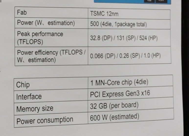
Let’s start with the package, which comes in at 7225 mm2. This is a typical BGA package, with other 6457 pins. Within the package are four silicon die, built on TSMC 12FFC, each of them 756.7 mm2 (32.2 mm x 23.5 mm), which means that this processor totals 3026.8 mm2 of silicon. That’s a far cry from the 800 mm2 of silicon used in high-end compute GPUs, or even the 1000 mm2+ used in high-end EPYC CPUs. Fundamentally this is an astonishing number to get your head around, especially for something that is meant to go onto a PCIe card.
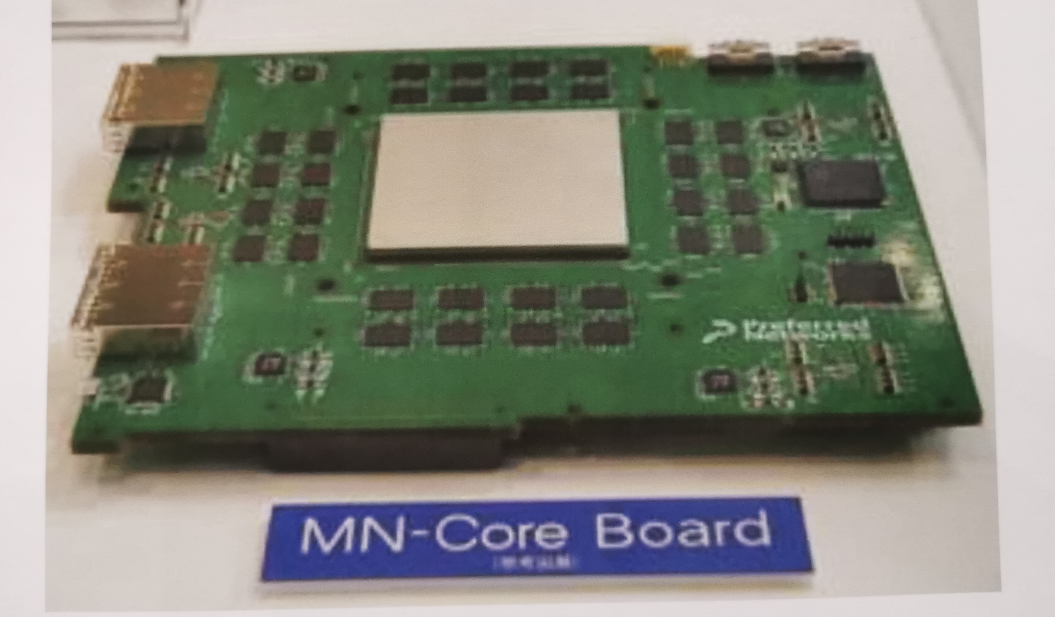
With the associated heatspreader, the chip sits on the PCB surrounded by 32 GiB of some form of memory. The whole device is a deep learning accelerator, aiming to provide key targets for performance and power. At 524 TeraFLOPs of half-precision (FP16) performance, the chip also has a 500W TDP, which means the goal of the chip was met: 1.05 TFLOPs per watt. At 0.55 V, it means the chip is pulling close to 1000 amps at load, and as a result a custom PCB design was required, but still is enabled through PCIe. The card is an extended PCIe design, with forced cooling (even in a server), and will sit in a 7U rack-mount chassis. Each server is a dual socket CPU with up to four of these cards, providing 2 PetaFLOPs of half-precision DL compute. With the cooling on the card, we are now up to 600W per card, and this is how it is calculated inside a server.

The chip is built as part of the MN-Core family. Preferred Networks is a company that specialises in building private supercomputers with specific needs. Since the founding in 2014, it has built $130m of funding, with almost $97m of it coming from Toyota. Preferred Networks has built three AI supercomputers for Tokyo University since 2017, mostly with P100 and V100 NVIDIA accelerators, with the latest MN-2 using 1024 V100 SXM2 parts to hit 128 PetaFLOPs total. This new chip is at the center of Preferred Networks’ latest MN-3 supercomputer, and will be the first with custom silicon.
MN-3 will have four of these chips per 7U server, giving ~2.1 PF of performance. There will be four servers to a rack, and about 300 racks, which comes to 4800 MN-Core boards. This would give 2.5 ExaFLOPs of total half-precision peak performance. David Schor at Wikichip estimates the total power consumption around 3.36 megawatts, which is mightily more efficient than other systems in the market. MN-3 is expected to go into operation in 2020.
David has also done some digging as to how this chip came to be. On our photos, we can clearly see the phrase ‘GRAPE-PFN2’ on the silicon, which stands for GRAPE, the name of Tokyo University’s internal silicon projects, and PFN2, or Preferred Networks. Tokyo U has a number of custom silicon projects under the GRAPE banner: one for gravitational calculations, one for many body calculations, one for molecular dynamics, etc, and it turns out that the Preferred Networks team was initially part of the GRAPE-DR physics co-processor project, and this is why the diagram of the architecture shown at Supercomputing looks so similar.
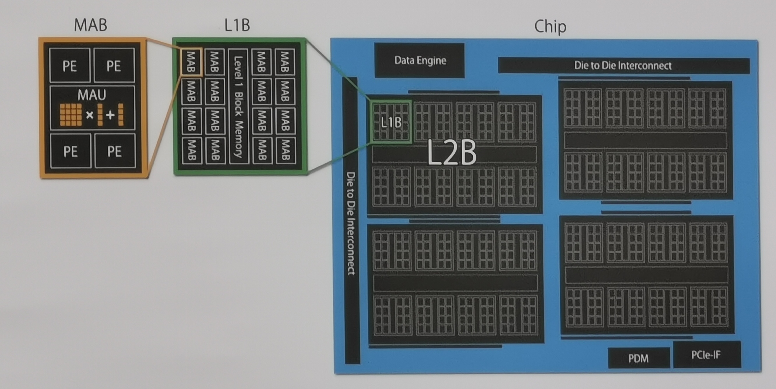
Each chip consists of two die-to-die interconnects, partnered with some scheduling engines, PCIe fabric, and the compute happens in four big ‘Level 2 Blocks (L2Bs)’. Each L2B features eight L1Bs and a shared cache, and inside in L1B are sixteen Matrix Arithmetic Blocks (MABs) as well as an L1 shared cache. Each MAB has four processing engines (PEs) as well as a matrix arithmetic unit (MAU), which seems built to perform matrix multiplication and addition. Altogether, one die will have 512 MABs, consisting of 2048 PEs and 512 MAUs. A whole chip would therefore have 2048 MABs, 8192 PEs, and 2048 MAUs. Keep scaling up and it becomes apparent how the high performance numbers could be achieved. Normally all of these units work in 16-bit, although combining PEs means that higher order precision can be achieved.
Preferred Networks has no plans to sell these chips or servers commercially. They have a specific customer in mind, and are likely building the software stack with deep integration with that partner. But still, 3000 mm2 of silicon per chip? 500W per chip? Insane.


17 Comments
View All Comments
extide - Friday, December 6, 2019 - link
Looks like each L2B has it's own memory controllers -- but that would only give each L2B a 64-bit wide memory IF, unless it's all ganged up somehow.Interesting.
brucethemoose - Friday, December 6, 2019 - link
That's a bizarre PCie card. Double height, with *2* x16 plugs that are physically detached from the main PCB... And wouldn't forced induction with a big axial fan be more power efficient than that little leaf blower?brucethemoose - Friday, December 6, 2019 - link
*forced airflow*deil - Friday, December 6, 2019 - link
they managed to make it incredibly uglyrpg1966 - Friday, December 6, 2019 - link
Yes, because looks are the number one priority for this card.rahvin - Monday, December 9, 2019 - link
The dual connections are probably not data related and are tied only to the power draw.MATHEOS - Friday, December 6, 2019 - link
where have you gone anandtech for so many yearsit's a shame about this achievement
Ryan Smith - Friday, December 6, 2019 - link
Where have we gone? We're still here.boozed - Friday, December 6, 2019 - link
That reads like a spambot padding its post count with innocuous nonsenseskavi - Friday, December 6, 2019 - link
lol what