Intel Launches Atom P5900: A 10nm Atom for Radio Access Networks
by Ryan Smith on February 24, 2020 9:10 AM EST
Continuing Intel’s run of Mobile World Congress-released announcements this morning, the chip maker is also announcing an interesting product in the form of a mobile-related Atom. Dubbed the Atom P5900, according to Intel the new chip has been designed specifically for radio access networks, wireless base stations, and similar devices, incorporating Intel’s Tremont Atom cores along with a series of hardware accelerators.
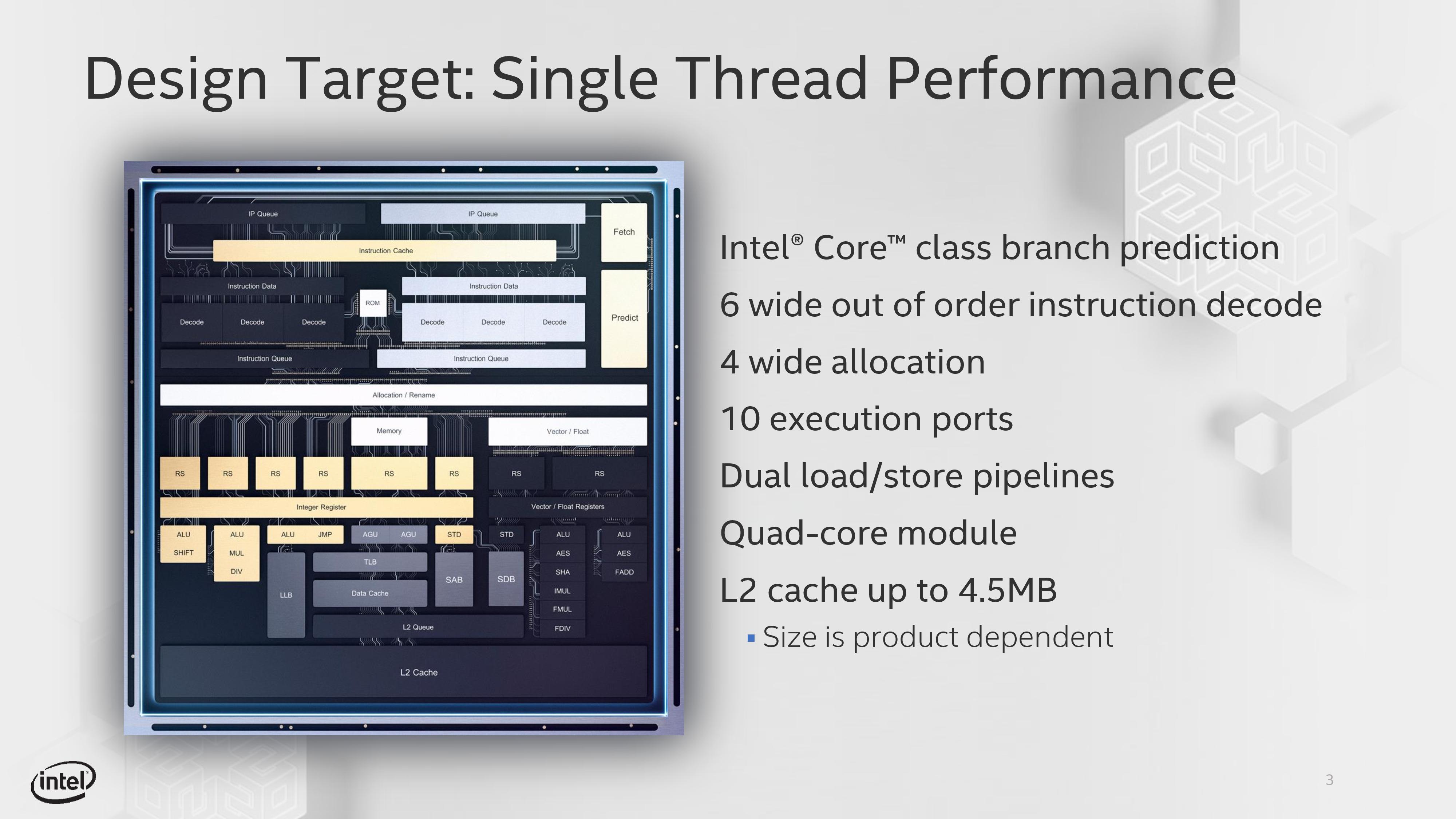
Formerly known as Snow Ridge, the Atom P5900 is one of the first chips based on Intel’s Tremont Atom cores. Designed around Intel’s 10nm process, Tremont is the next-generation Atom, designed to be wider and more performant than any Atom CPU core before them. But more interesting and relevant to the market at hand, the new chip also has several network acceleration functions, including integrated packet processing, which help to make it a specialized chip for networking deployments. The chip is by and large the successor to the previous Atom C-series, though with even more of a networking focus.
Intel’s primary market for the chip is for operating cellular base stations, where the company thinks they can win off a combination of high power efficiency and high throughput, especially when the accelerators can be used. That said, Intel also has significant edge computing ambitions in general, so depending on just how flexible the chip is and what markets Intel decides to chase, it could pop up in more places.
According to Intel, base stations using the new Atom will begin to be deployed this year. With deals already lined up with Ericsson, Nokia, and ZTE, the company is hoping to make a quick-but-lasting impact on the radio access network market.
Update 2/25: Some questions had been floating around as to whether Snow Ridge was one of Intel's drivers for its Foveros technology, given some old Snow Ridge slides that contained the same pictoral representations as those used in the initial Foveros announcement. Intel has confirmed that the Snow Ridge Atom P5900 does not contain any EMIB of Foveros technology.
Source: Intel


16 Comments
View All Comments
anonomouse - Monday, February 24, 2020 - link
Looks like it scales up to 24 cores/2.2ghz/27mb “cache” although it’s not clear how that cache total is organized: https://www.intel.com/content/www/us/en/products/p...qap - Monday, February 24, 2020 - link
Thanks for the link. Thats quite impressive for atom. And it is getting very wide compared to first atoms. 6-wide OoO is Sandy Bridge territory and most likely higher IPC thanks to newer instruction set. This will most likely be directly comparable to 12-16 big cores (where it can get most of parallelism).Wilco1 - Monday, February 24, 2020 - link
It has 2 sets of 3-wide decoders. In straight-line code it can only decode 3 instructions per cycle. For branchy code the 2nd decoder reduces latency and helps filling unused decode slots, but that doesn't make it 6-wide. It has 4-wide rename so even if the decoder could produce 6 instructions, it could process only 4.It's definitely the fastest Atom so far, but like all its predecessors, it remains lacklustre. At just 2.2 GHz (no turbo!), no AVX, no SMT, it would take ~3 of these to match 1 big core...
yeeeeman - Tuesday, February 25, 2020 - link
I agree. Hence the choice of 4 Tremont cores and one sunny cove core in Lakefield.ProDigit - Monday, July 6, 2020 - link
Not needed if you are ok with the 2GHz it offers. It's faster than a Raspberry Pi 4b per core, and it has up to 24 of them instead of 4.For Boinc, FAH, or other data crunching, the 24 core could probably outdo a 9th gen Core i5 (4/8 CPU/threads) in all core load.
HStewart - Monday, February 24, 2020 - link
Thanks for the link. I am curious about two thing1. Is this basically tremont processor
2. is this serious e basically the successful for C series chips like the C3955
https://ark.intel.com/content/www/us/en/ark/produc...
HStewart - Monday, February 24, 2020 - link
Never mind - article states it - but it does state it.DanNeely - Monday, February 24, 2020 - link
Those numbers imply 1MB + 128kB/core; although partitioning into 3 levels is certainly possible. Do we know anything about Tremont in general?Wilco1 - Monday, February 24, 2020 - link
Yes, according to https://www.anandtech.com/show/15009/intels-new-at... 27MB for 24 cores looks like 6 4-core modules with a shared 4.5MB L2 cache. So no L3.anonomouse - Wednesday, February 26, 2020 - link
Interesting wrinkle here though: https://www.intel.com/content/www/us/en/products/p..."L2 Cache of 4.5MB per 4-core cluster and shared LLC cache up to 15MB"
The L2 matches up, but this supposed shared LLC doesn't seem to show up anywhere.