TSMC Preps 6x Reticle Size Super Carrier Interposer for Extreme SiP Processors
by Anton Shilov on May 26, 2023 3:15 PM EST- Posted in
- Semiconductors
- HPC
- TSMC
- AI
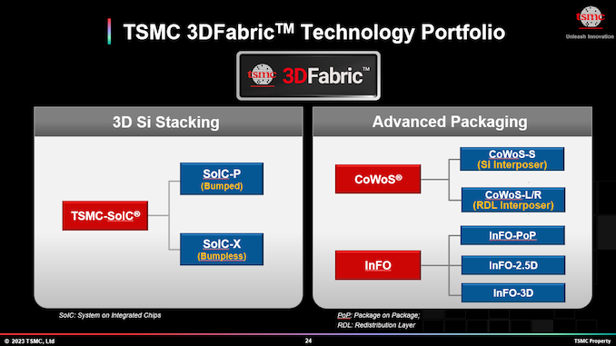
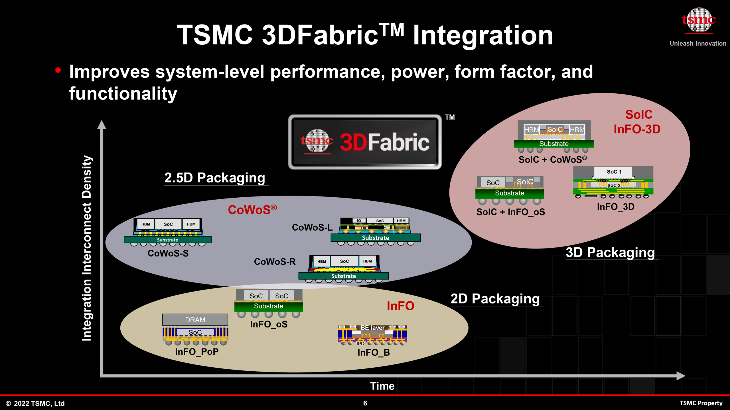
- CoWoS-L
As part of their efforts to push the boundaries on the largest manufacturable chip sizes, Taiwan Semiconductor Manufacturing Co. is working on its new Chip-On-Wafer-On-Substrate-L (CoWoS-L) packaging technology that will allow it to build larger Super Carrier interposers. Aimed at the 2025 time span, the next generation of TSMC's CoWoS technology will allow for interposers reaching up to six times TSMC's maximum reticle size, up from 3.3x for their current interposers. Such formidable system-in-packages (SiP) are intended for use by performance-hungry data center and HPC chips, a niche market that has proven willing to pay significant premiums to be able to place multiple high performance chiplets on a single package.
"We are currently developing a 6x reticle size CoWoS-L technology with Super Carrier interposer technology," said said Yujun Li, TSMC's director of business development who is in charge of the foundry's High Performance Computing Business Division, at the company's European Technology Symposium 2023.
Global megatrends like artificial intelligence (AI) and high-performance computing (HPC) have created demand for seemingly infinite amounts of compute horsepower, which is why companies like AMD, Intel, and NVIDIA are building extremely complex processors to address those AI and HPC applications. One of the ways to increase compute capabilities of processors is to increase their transistor count; and to do so efficiently these days, companies use multi-tile chiplet designs. Intel's impressive, 47 tile Ponte Vecchio GPU is a good example of such designs; but TSMC's CoWoS-L packaging technology will enable the foundry to build Super Carrier interposers for even more gargantuan processors.
The theoretical EUV reticle limit is 858mm2 (26 mm by 33 mm), so six of these masks would enable SiPs of 5148 mm2. Such a large interposer would not only afford room for multiple large compute chiplets, but it also leaves plenty of room for things like 12 stacks of HBM3 (or HBM4) memory, which means a 12288-bit memory interface with bandwidth reaching as high as 9.8 TB/s.
"The Super Carrier interposer features multiple RDL layers on the front as well as on the backside of the interposer for yield and manufacturability," explained Li. "We can also integrate various passive components in the interpreter for performance. This six reticle-size CoWoS-L will be qualified in 2025"
Building 5148 mm2 SiPs is an extremely tough tasks and we can only wonder how much they will cost and how much their developers will charge for them. At present NVIDIA's H100 accelerator, whose packaging spans an interposer multiple reticles in size, costs around $30,000. So a considerable larger and more powerful chip would likely push prices higher still.
But paying for the cost of large processors will not be the only huge investments that data center operators will need to make. The amount of active silicon that 5148 mm2 SiPs can house will almost certainly result in some of the most power-hungry HPC chips produced yet – chips that will also need equally powerful liquid cooling to match. To that end, TSMC has disclosed that it has been testing on-chip liquid cooling technology, stating that it has managed to cool down silicon packages with power levels as high as 2.6 kW. So TSMC does have some ideas in mind to handle the cooling need of these extreme chips, if only at the price of integrating even more cutting-edge technology.


2 Comments
View All Comments
FunBunny2 - Friday, May 26, 2023 - link
so. where is ARM in this arms race?nandnandnand - Friday, May 26, 2023 - link
What?https://www.anandtech.com/show/14914/arm-tsmc-demo...