Rapidus Wants to Supply 2nm Chips to Tech Giants, Challenge TSMC
by Anton Shilov on July 26, 2023 1:00 PM EST- Posted in
- Semiconductors
- IBM
- GAAFET
- 2nm
- Rapidus
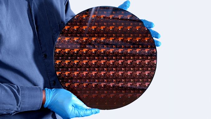
It has been a couple of decades since a Japanese fab has offered a leading-edge chip manufacturing process. Even to this day, none of the Japanese chipmakers have made it as far as adopting FinFETs, something that U.S. and Taiwanese companies adopted in early-to-mid-2010s. But Rapidus, a semiconductor consortium backed by the Japanese government and large conglomerates, plans to leapfrog several generations of nodes and start 2nm production in 2027. Interestingly, the company aims to serve world's leading tech giants, challenging TSMC, IFS, and Samsung Foundry.
The endeavor is both extremely challenging and tremendously expensive. Modern fabrication technologies are expensive to develop in general. To cut down its R&D costs, Rapidus teamed up with IBM, which has done extensive research in such fields as transistor structures as well as chip materials. But in addition to developing a viable 2nm fabrication process, Rapidus will also have to build a modern semiconductor fabrication facility, which is an expensive venture. Rapidus itself projects that it will need approximately $35 billion to initiate pilot 2nm chip production in 2025, and then bring that to high-volume manufacturing in 2027.
To recover the massive R&D and fab construction costs, Rapidus will need to produce its 2nm chips in very high volumes. As demand from Japanese companies alone may not suffice, Rapidus is looking for orders from international corporations like Apple, Google, and Meta.
"We are looking for a U.S. partner, and we have begun discussions with some GAFAM [Google, Apple, Facebook, Amazon and Microsoft] corporations," Atsuyoshi Koike, chief executive of Rapidus, told Nikkei. "Specifically, there is demand [for chips] from data centers [and] right now, TSMC is the only company that can make the semiconductors they envision. That is where Rapidus will enter."
Despite escalating chip design costs, the number of companies opting to develop their own custom system-on-chips for artificial intelligence (AI) and high-performance computing (HPC) applications is growing these days. Hyperscalers like AWS, Google, and Facebook have already developed numerous chips in-house to replace off-the-shelf offerings from companies like AMD, Intel, and NVIDIA with something that suits them better.
These companies typically rely on TSMC since the latter tends to offer competitive nodes, predictable yields, and the ability to re-use IP across various products. So securing orders from a tech giant is challenging for a new kid on the block. But Rapidus' strategy is not completely unfounded, as the number of hyperscalers that need custom silicon is growing and one or two may opt for Rapidus if the Japanese company can provide competitive technology, high yields, and fair pricing.
With that said, however, Rapidus is also making it clear that the company does not plan to emulate TSMC's entire business model, where they'd serve a wide range of clients like TSMC does. Instead, Rapidus intends to start with about five customers, then gradually expand to 10, and then see if it wants and can serve more.
"Our business model is not that of TSMC, which manufactures for every client," said Koike. "We will start with around five companies at most, then eventually grow to 10 companies, and we'll see if we'll increase the number beyond that."
It is unclear whether such a limited client base can generate enough demand and revenue to recover Rapidus' massive investment needed to kick-start 2nm production by 2027. It is also going to be a challenge to secure even five significant 2nm orders by 2027 given the limited number of companies ready to invest in chips to be made on a leading-edge technology and competition from established players like TSMC, Samsung Foundry, and IFS.
However, from the Japanese government's perspective, Rapidus is seen as a catalyst for revitalizing Japan's advanced semiconductor supply chain, rather than a money making machine in and of itself. So even if the 2nm project was not an immediate success, it can be justified as a stepping stone towards creating more opportunities for local chip designers.
As for revenue, Koike predicts that quotes for its 2nm chips will be 10 times greater than for chips currently made by Japanese firms, which is of course a significant change for the Japanese chip industry. This is not particularly surprising though, as the most advanced process technology available in Japan today is 45nm, which these days is a very inexpensive node as it is used on fully depreciated fabs and does not require any new equipment.


19 Comments
View All Comments
meacupla - Wednesday, July 26, 2023 - link
This is an overly ambitious project from a country that has had numerous overly ambitious projects fail on them in recent years.My money is on this project failing within 10yrs, and I like my odds.
- They have no expertise at 2nm node fabrication. They will have to import all labor from IBM, until they can get highly skilled workers trained for the task.
- They are building the fab in a location that has never had semiconductor manufacturing, ever. So (Chitose, Hokkaido) So all skilled, domestic workers would have to be transferred over. Assuming there are any to spare.
- The group of companies funding this corporation are deeply at odds with 2nm process. Literally, none of them benefit from having 2nm. Maybe Kioxia can for SSD controllers. Can NAND even be made on 2nm?
Denso, MUFG Bank, NEC, NTT, Softbank, Sony? They don't even make design semiconductors themselves, let alone something that needs 2nm.
Toyota? Why would a car maker need 2nm chips for their cars? Most of that stuff is made on >28nm. Jumping to 14nm would be a huge leap already, and they wouldn't need all the added complexity of gluing a 2nm chip to a substrate.
- This is fresh off the heels of Toyota's MIRAI, and Mitsubishi's SpaceJet. Both were overly ambitious projects at domestic manufacturing, and miserable failures.
- Then there is the 2000~2010 version of Rapidus, which is called "Project ASUKA". That too, was a miserable failure. And guess what same mistakes are being made?
Samus - Thursday, July 27, 2023 - link
-Nobody has expertise at 2nm. It doesn't exist yet. Everyone is at equilibrium in this regard so having skilled workers is irrelevant when any company developing next-gen fab processes would need to train technicians anyway.-Japan, like most educated industrialize nations, has plenty of domestic talent. Japanese-made products ranging from vehicles to construction to whiskey are all considered among the best in the world, with class-leading quality control, should be evidence enough there will no little trouble filling shoes for fab operators and engineers.
-True the group of companies backing this product have little demand for the products themselves, but as conglomerates, their purpose isn't to buy products they invest in, but profit from them. Softbank is a classic example of this, but most of the investors are just that, investors. You won't see SSD controllers built on 2nm - this node is for HPC not rudimentary ASICs. Next gen SSD controllers are built on, at best, TSMC's 12nm. 3 generations old. There is no benefit for simple silicon to be tapped on such an expensive node. The same goes for virtually every chip in a vehicle or consumer electronic. Perhaps someday with self driving AI there will be demands for bleeding edge performance processors at 2nm in vehicles but it wont be for another decade.
-Toyota MIRAI and Mitsu SpaceJet had little outside funding as low-demand ambitions. The Japanese government was the sole investor for both. Rapidus is different as there are many hands in the cookie jar and if one entity pulls out, it wont crumble.
-I have no idea what you are talking about "project asuka" but Elpida\NEC\Mitsubishi\Hitachi were heavily hit by the world financial crisis in 2008-2009. The Fukushima disaster shortly after, costing far more than the Japanese government let on (speculation) didn't help and prevented a bailout of the Japanese semiconductor industry which essentially went bankrupt by 2012.
There is so much riding on Rapidus success' (even the US government has interest in its success for national security and supply chain diversification) that it is unlike any Japanese investment project in recent history.
But I agree it is ambitious and incredibly challenging to try to catch up to TSMC, which has an enormous market cap, massive government subsidization and an established client list with known knowns regarding yields and timetables. The thing is, when (not if) China invades Taiwan, TSMC becomes irrelevant.
mattbe - Friday, July 28, 2023 - link
"Nobody has expertise at 2nm. It doesn't exist yet. Everyone is at equilibrium in this regard so having skilled workers is irrelevant when any company developing next-gen fab processes would need to train technicians anyway."Haha "equilibrium". notwithstanding that you used the wrong word here, are you assuming that the experiences acquired by Intel, Samsung and TSMC are irrelevant when it comes to implementing a cutting edge node?
Like I have a hard time understanding your logic. You are basically saying it's fine to skip everything in between because you are building a new node.. Well's how are you even going to do it without even having worked on a simpler node?
Eliadbu - Friday, July 28, 2023 - link
True his take is very dumb one. what enables TMSC Samsung and Intel to develop those cutting edges are decades of knowledge, expertises, technology, patents, know-how, skill etc. building new nodes is building on past experience to create something better. unless this Rapidus get the people with those expertises ,license patents and technology from some company like how GLO-FO licensed 14nm from Samsung, this (very) expensive endeavor is doomed to fail. They are probably better license several nodes before even trying to create their own high end nodes. With that said I do wish them the best of luck and I would love to be proven wrong in this case - despite me not seeing this happen. I think the best outcome for them would be something like intel 10(7) process that was delayed for years until we got it in the market.Samus - Sunday, July 30, 2023 - link
I guess my 20 years working at Argonne National Laboratory as a physicist at the APS means I know nothing then. You keyboard warriors are correct. My take is indeed dumb and I am using the wrong words. Clearly you guys know so much more than I do throwing company names around and talking about previous gen nodes influencing the development of next gen nodes. You should have my job, and I can work at McDonalds where I belong.meacupla - Sunday, July 30, 2023 - link
Assuming you are serious, I don't understand how you think your specialty in, presumably, particle physics, has anything to do with building a successful fab in Japan.I would assume that you need to be able to at the very least read Japanese, so you can get some info on history, socioeconomic, and engineering.
and since you asked what is Project Asuka, here is some of it: https://www.jeita.or.jp/cgi-bin/topics/detail.cgi?...
But the gist of it was designing and fabricating devices for a Japanese domestic SoC. Starting in 2001 and ending in 2011.
And seeing as there is no Japanese SoC, we can see that this failed.
Samus - Thursday, August 3, 2023 - link
You would be surprised how much "particle physics" has to do with manufacturing transistors. IBM has 3 sectors at the APS ring and most of their recent manufacturing breakthroughs are directly related to the research done here. In fact it was IBM and the Alpha 6 team that won AMD the contract for the terabyte storage facility based on the Athlon architecture over 20 years ago here. The Aurora is its spiritual (though not direct) successor.It all starts somewhere, and a lot of it starts here, in education and government. Ask TSMC. I don't need to work at a fab to realize that. We are the precursor to the fab: fabs don't do R&D, we do. They are built on the theories tested here. Intel knows this all too well. The failures that happened at Fermi were one of the hiccups blockading them from moving forward for years as they couldn't stop leakage with the gate sizes and materials they were using, but business politics made it worse with poor team management and redundant data collection from multiple facilities.
Santoval - Wednesday, July 26, 2023 - link
I was not aware the Japanese do not even fab FinFET wafers yet.Since their target node is 2nm (whatever that might mean in transistor density, which is the crucial metric) I assume they're also going to skip FinFETs and move directly to some GAA-FET variant.
A tech TSMC is currently still developing and, I believe, Samsung is now sampling. "Ambitious project" is quite an understatement. Big bucks alone are not enough; they require expertise and a truckload of ASML EUV scanners if they're to reach a meaningful capacity.
Both are very hard to get, but if they have enough funds they might lure some talent away from the established big players.
Blastdoor - Thursday, July 27, 2023 - link
Big bucks are not enough — you also need the things that big bucks can buy. As Homer Simpson once observed, money can be exchanged for goods and services.ABR - Thursday, July 27, 2023 - link
Geopolitical supplier diversification will be a clear driver for them to get customers but ease will depend on how far Intel gets in this space by the time (if) they come online. But Japan, as the US, has realized that advanced chip manufacturing is increasingly a fundamental capability in the world economic arena and therefore is willing to make a sizeable investment. The motivation for the private partners is less clear, as there are surely easier ways to make a buck.