Samsung Details Exynos 5 Octa Architecture & Power at ISSCC '13
by Anand Lal Shimpi on February 20, 2013 12:42 PM EST- Posted in
- SoCs
- Samsung
- Arm
- Cortex A15
- Cortex A7
- exynos 5 octa
At CES this year Samsung introduced the oddly named Exynos 5 Octa SoC, one of the first Cortex A15 SoCs to implement ARM's big.LITTLE architecture. Widely expected to be used in the upcoming Galaxy S 4, the Exynos 5 Octa integrates 4 ARM Cortex A7 cores and 4 ARM Cortex A15 cores on a single 28nm LP HK+MG die made at Samsung's own foundry. As we later discovered, the Exynos 5 Octa abandons ARM's Mali GPU for Imagination's PowerVR SGX 544MP3, which should give it GPU performance somewhere between an iPad 3 and iPad 4.
The quad-core A7 can run at between 200MHz and 1.2GHz, while the quad-core A15 can run at a range of 200MHz to 1.8GHz. Each core can be power gated independently. The idea is that most workloads will run on the quad-core A7, with your OS hot plugging additional cores as performance demands increase. After a certain point however, the platform will power down the A7s and start switching over to the A15s. Both SoCs implement the same revision of the ARM ISA, enabling seamless switching between cores. While it's possible for you to use both in parallel, initial software implementations will likely just allow you to run on the A7 or A15 clusters and switch based on performance requirements.
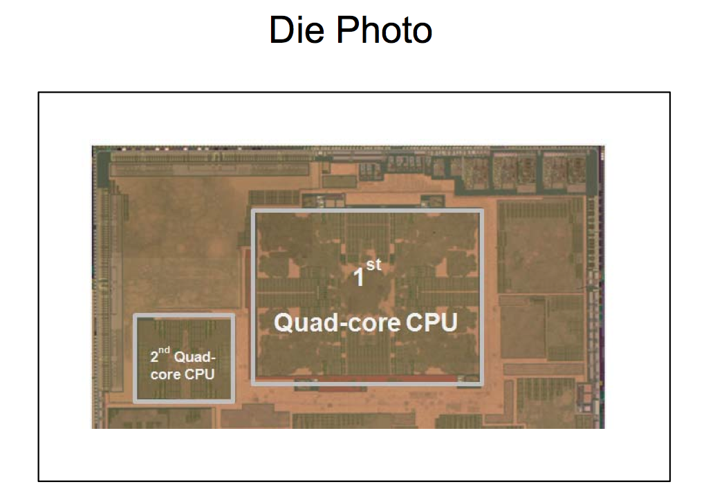
What's most interesting about Samsung's ISSCC presentation is we finally have some hard power and area data comparing the Cortex A15 to the Cortex A7. The table above puts it into numbers. The quad-core A15 cluster occupies 5x the area of the quad-core A7 cluster, and consumes nearly 6x the power in the worst case scenario. The area difference is artificially inflated by the fact that the A15 cluster has an L2 cache that's 4x the size of the A7 cluster, but looking at the die photo below you can get a good feel for just how much bigger the A15 cores are themselves:
In its ISSCC presentation, Samsung stressed the value of its custom libraries, timing tweaks and process technology selection in bringing the Exynos 5 Octa to market. Samsung is definitely marching towards being a real player in the SoC space and not just another ARM licensee.
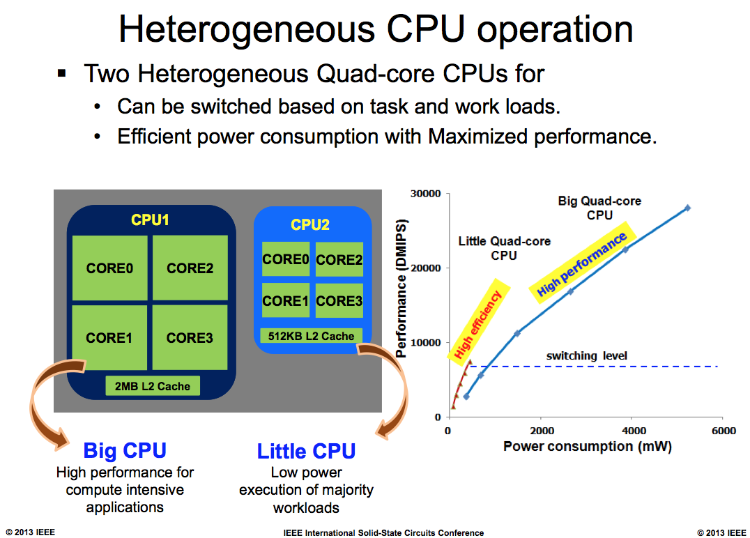
The chart below is one of the most interesting, it shows the relationship between small integer code performance and power consumption on the Cortex A7 and A15 clusters. Before switching from the little CPU to the big one, power consumption is actually quite reasonable - south of 1W and what you'd expect for a smartphone or low power tablet SoC. At the lower end of the performance curve for the big CPU things aren't too bad either, but once you start ramping up clock speed and core count power scales linearly. Based on this graph, it looks like it takes more than 3x the power to get 2x the performance of the A7 cluster using the Cortex A15s.


52 Comments
View All Comments
alex3run - Wednesday, February 20, 2013 - link
And where is the official information about the GPU and it's power consumption?rd_nest - Wednesday, February 20, 2013 - link
http://www.theinquirer.net/inquirer/news/2249399/s...toyotabedzrock - Wednesday, February 20, 2013 - link
That does not sound like a sgx gpu.I think they should find a gpu that supports opengl es 3
rd_nest - Wednesday, February 20, 2013 - link
72GFlops..Most probably T604. Was same for N10.lmcd - Sunday, February 24, 2013 - link
I think it's pretty obviously an ARM solution as that's what they have experience with. I think that also makes more sense because they have been touting the benefits of using those combinations. Furthermore the 544MP3 would practically be a step back from the T604, even ignoring the other ARM and IT solutions they could use.Their rep probably got it wrong.
banvetor - Wednesday, February 20, 2013 - link
One of the unanswered questions at ISSCC was what is the delay penalty from switching between the A7 and the A15 cores... I don't see all that bright future for this baby.StormyParis - Wednesday, February 20, 2013 - link
Why ? because of a switching delay you don't know, for a switch you don't know the frequency of ?jeffkibuule - Wednesday, February 20, 2013 - link
I don't think the delay switch matters that much, when the goal of these chips is reasonable performance with good battery life, not maximum performance, otherwise you much as well just chuck the A7 cores and run the A15s at full blast.twotwotwo - Wednesday, February 20, 2013 - link
Yeah, the compromise-y nature of it is important for the whole thing to make sense. In theory, 6W's a lot. In real use, you rarely hit that--you usually just blast 1-2 of the A15s for a few seconds while you load a webpage or app or do some other big chunk of CPU-bound work.If I'm going to second-guess and play armchair engineer (as DigitalFreak aptly put it), maybe you can imagine other uses for all that die area than going 4+4-core when many workloads still aren't heavily threaded--more cache w/the A15s, more GPU (I bet games on 1080p phone screens can use a lot), something. Apple was OK with dual-core, at least as of the A6(X). Other hand, I haven't the first clue how other designs perform, etc. and Samsung does, so I should close my mouth. :)
wsw1982 - Wednesday, February 20, 2013 - link
I don't see the mansion of L3 cache, and the L2 cache of A7 and A15 are not shared. Therefore, it's highly possible the switch is across the main memory, which may add mile-seconds of delay (dumping and reloading cache data to and from low power ddr, power down and warm up the cores). How much should A15/A7 done to just even out of the performance and energy penalty of switching?