Update: AMD Announces Radeon M300 Series Notebook Video Cards
by Ryan Smith on May 6, 2015 7:20 PM EST- Posted in
- GPUs
- AMD
- Radeon
- AMD FAD 2015
Along with a bevy of roadmap announcements at financial analyst day, AMD has also slipped in a full-on mobile GPU announcement today at the event.
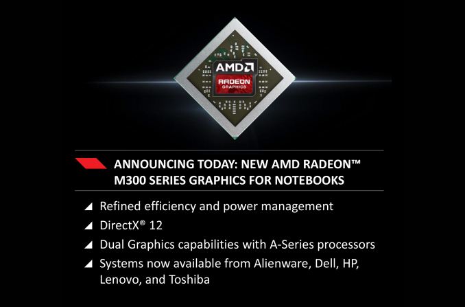
Being announced today is the Radeon M300 series. With so much other news coming out of FAD we’re still tracking down more information on the product line, but of the information released by AMD so far, we do know that these parts are being advertised as refined parts with better efficiency and power management. AMD’s FAD presentation has not made any mention of what specific GPUs are being used here or of specific SKUs (we may yet see a press release), so it’s not clear whether there are new GPUs involved or if these are simply rebadges of existing GPUs and products.
AMD does note that M300 systems should already be available from several of AMD’s usual partners, including Alienware, HP, Dell, Lenovo, and Toshiba. Meanwhile given the timing of the announcement and the fact that AMD is specifically advertising these GPUs as supporting Dual Graphics mode with AMD’s A-series APUs, I suspect some of these GPUs may be intended to work alongside AMD’s Carrizo APU, which is due this year.
Update: AMD has since released the details of the M300 SKUs on their website, and though they’re not incredibly detailed, they give us an idea of just what AMD is up to.
| AMD M300 Series GPU Specification Comparison | |||||
| R9 M375 | R7 M360 | R5 M330 | |||
| Was | Variant of R9 M270/M260 | Variant of R7 M270/M260 | Variant of R5 M255 | ||
| Stream Processors | 640 | 384 | 320 | ||
| Texture Units | 40 | 24 | 20 | ||
| ROPs | 16 | 4? | 4? | ||
| Boost Clock | <=1015MHz | <=1015MHz | <=1030MHz | ||
| Memory Clock | 2.2GHz DDR3 | 2GHz DDR3 | 2GHz DDR3 | ||
| Memory Bus Width | 128-bit | 64-bit | 64-bit | ||
| VRAM | <=4GB | <=4GB | <=4GB | ||
| GPU | Cape Verde | Oland | Oland | ||
| Manufacturing Process | TSMC 28nm | TSMC 28nm | TSMC 28nm | ||
| Architecture | GCN 1.0 | GCN 1.0 | GCN 1.0 | ||
Unfortunately it looks like everything is going to be a rebadge/rehash of AMD’s existing GCN 1.0 GPUs. While AMD’s specs do not confirm which GPUs we’re looking at, and hence we’re admittedly taking an educated guess, based on the specs and features we have every reason to believe we’re looking at Cape Verde and Oland, the two GPUs that also backed AMD’s M200 series. I had been hoping for a cut-down Bonaire in here, to bring GCN 1.1 to mobile, but it doesn’t look like that’s in the cards.
What we have then is a 3 product stack with some very unusual configurations. Compared to their M200 counterparts, all 3 M300 parts have much higher GPU clockspeeds. AMD is now allowing clockspeeds over 1GHz, even for the low-end M330. Though as always, we need to remind everyone that these are “up to” speeds, and OEMs get the final choice in what the shipping clockspeed of a M300 part will be in any given laptop.
And although clockspeeds are up, memory bandwidth is way, way down. All of these parts ship with DDR3, and of those only the M375 gets a 128-bit memory bus. The other two parts, based on Oland, are shipping with a 64-bit memory bus. On the M200 series AMD was using GDDR5 with Cape Verde and the full 128-bit memory bus with Oland, so these new parts have half (or less) of the memory bandwidth of their M200 counterparts. The fact that AMD did this while increasing clockspeeds (which generally has a knock-on impact on power consumption) is very odd, and I would expect that these new parts are going to be bandwidth starved and will not reach the full potential of their respective GPUs. Meanwhile there's also some uncertainty over the number of ROPs enabled on the M360 and M330; with 64-bit memory buses on a chip that natively has a 128-bit memory bus, AMD may have disabled half of the ROPs in the process.
Looking at these parts overall, in AMD’s FAD event today the company specifically noted the dual graphics capabilities of the M300 series, and I suspect that’s precisely what these parts are meant for. They’re not intended to be stand-alone, but rather they’re designed to be paired with Carrizo/Kaveri APUs to inject more graphics silicon to improve GPU performance. In which case we’re looking at another wrinkle in performance, not only from dual graphics but from the fact that AMD’s APUs tend to be hungry for bandwidth as well, in which case the impact of these slower memory buses may not be as great.
Finally, it’s interesting to note that AMD only went up to M375 here. They did not introduce an M380 or M390 series part, not even rebadging the Pitcairn/Tonga parts that compose the faster members of the M200 series. This may be a sign that AMD intends to introduce faster parts later on, but for the moment that’s merely speculation on my part.


37 Comments
View All Comments
testbug00 - Wednesday, May 6, 2015 - link
Guessing that Tonga m295x becomes the m390x. Cut down becomes m390. m380(x) is old m290(x)nathanddrews - Wednesday, May 6, 2015 - link
These are not likely to be straight rebadges if they claim "refined efficiency and power management". Something has to change physically to make that happen.testbug00 - Wednesday, May 6, 2015 - link
likely tweaked steppings for the most part. And Tonga taking a larger part of the high end cards.dragonsqrrl - Wednesday, May 6, 2015 - link
I'm guessing their plan is to phase out GCN 1.0 entirely (Pitcairn), like the desktop 300 series. That in itself would help a bit.dragonsqrrl - Wednesday, May 6, 2015 - link
Update: lol, nvm... wow that's really quite sad.chizow - Wednesday, May 6, 2015 - link
Yeah..those inventory problems are real.nathanddrews - Thursday, May 7, 2015 - link
Sheesh, that's pretty pathetic.chizow - Thursday, May 7, 2015 - link
Yeah, better than tossing them in a landfill and writing them off though, I guess.MrSpadge - Wednesday, May 6, 2015 - link
No, they can just choose a different working point (similar frequency, slightly lower voltage) to save power and claim a refinement. Would be nice if they did more, but since Tonga I'm not expecting anything from them anymore.Crunchy005 - Wednesday, May 6, 2015 - link
So basically what Nvidia did with the mobile 900 series right? O and the 950m with ddr3 and gddr5 under the same name to confuse people more.